|
STELLA NEWS SITE is managed by Stella Corporation Inc. |

|
FPD/PCB NEWS〜September 24
|
|
|
|
FPD/PCB NEWS〜September 21
|
|||
|
Housed on the center's first floor are a lab area for co-creation with business partners and a training center for customers. An open innovation area occupies a part of the first and second floors. Total floor area is 19,400 m2 (including ancillary facilities). |
|||

|
FPD/PCB NEWS〜September 13
|
|||
|
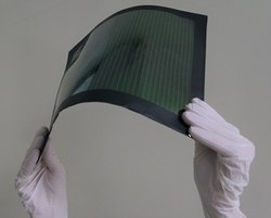
The company previously developed a two-step coating process that first applied a layer of PbI2 (lead iodide) ink to a substrate, followed by a layer of MAI (methyammonium iodide, CH3NH3I) ink, triggering a reaction that formed an MAPbI3 layer. However, this multi-step approach had a low coating rate and often left unreacted sections in the perovskite layer. The alternative is a one-step process that applies MAPbI3 ink directly, but it is not easy to control crystallization of the MAPbI3 and obtain a uniform perovskite layer across a large area. A new coating method that solves these problems was required. The company has developed a one-step meniscus coating method that uses improved ink, film drying processes and production equipment to form a uniform perovskite layer over an area as large as 703cm2. These innovations halve the steps for deposition of the perovskite layer, and raise the coating speed to 6 meters per minute on a 5×5 cm2 module, a rate that meets requirements for mass production. The company previously reported 703cm2 polymer film-based perovskite photovoltaic modules, the one-step meniscus coating method achieves a PCE of 15.1%, the world's highest ever for a polymer film-based large-area perovskite photovoltaic module. This higher PCE and the faster, simplified production process, significantly advance progress toward the commercialization of highly efficient, low-cost, polymer film-based perovskite photovoltaic modules. |
|||