|
STELLA NEWS SITE is managed by Stella Corporation Inc. |

38th NEPCON JAPAN (Jan. 24-26)
38th NEPCON JAPAN
Topics of printing process inclusive of screen-printing method were proposed
January 24-26, 38th NEPCON JAPAN was held in Tokyo Big Site. In this here, main topics about electronics are picked up.
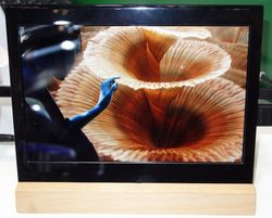
Natural 3D image is expressed by new TFT-LCD system
As concerns display module and system, OKAYA exhibited several TFT-LCD systems, such as high resolution TFT-LCD, reflection type TFT-LCD, and so on. Main exhibition was a specific glass-free 3D TFT-LCD monitor, was developed by psHolix (Switzerland). In this system, 3D image can be obtained without a specific glass by laminating a specific film on the front of TFT-LCD module. And also, it's possible to view natural 3D image without uncomfortable feeling from any angle. By the way, its release plan in Japan is not fixed yet.
Pic.1 3D TFT-LCD monitor without glass
Oxidation of Cu film is suppressed by Cu-Ni
With respect to material for electric device, Sumitomo Metal Mining proposed a Cu-Ni powder & ink. After coating and annealing in N2 environment, Nano size Cu and Ni are precipitated. Especially, Nano Ni are precipitated in the top plane. For this reason, its Ni layer functions as blocking layer of oxidation of Cu film. In short, oxidation of Cu is greatly suppressed. Its specific resistance is a few dozen μΩ・cm. Off course, it's possible to modify specific resistance and oxidation resistance by mixing ratio of Cu and Ni because of trade-off relationship. Typical anneal temperature is 250℃. And also, it's possible to correspond to wide range of viscosity, in a word, correspond various printing methods, such as, ink-jet printing method, screen printing method, and so on.
In the booth, printed samples of glass substrate and polyimide substrate. This ink can be adhered to these substrates in sure. By the way, this powder, ink, and coated substrate will be released from Sumitomo Metal Mining.
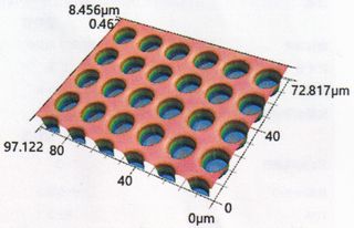
Low cured photosensitive polyimide is useful for midair encapsulation
Pic.2 Patterning image of Via pattern with 8μm diameterArakawa Chemical Industries proposed a photosensitive polyimide “PR-P1” for manufacturing process of MEMS and semiconductor.
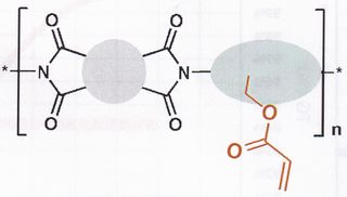
Fig 1. Molecule structure of PR-P1
Figure 1 shows molecule structure of PR-P1, is a ring-closing polyimide with UV reaction group. After UV exposure, it can be patterned by development using organic solvent, such as cyclopentanone. And also, it can exposured by irradiation of ghi line. Furthermore, it can be cured at very low temperature, same as 115℃ because of ring-closing structure. In short, solvent is vaporized in curing process. Of course, after coating and curing, high thermal resistance, strong property, and low thermal expansion are obtained because of basial characteristics of PI.
As above, it's useful for midair encapsulation of MEMS and semiconductor. Picture2 shows patterning image of Via pattern with 8μm diameter. It can be finely patterned easily.
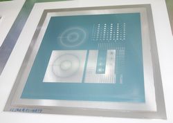
Screen mask is directly patterned by direct imaging system
Total supplier of screen printing, Seria Corporation appealed a direct imaging (DI) system “DLE(Digital Light Engraver) Compact” for manufacturing of DI screen mask. It's developed by CST (Switzerland). In this system, photosensitive emulsion is directly (photomask-free) exposured by patterned UV light, is patterned by DLP (Digital Light Prosessing) method using DMD array. It's relatively reasonable same as 40 - 50 million yen. Imaging resolution is 5080 dpi at the maximum. It's possible to pattern at L&S = 50/50 μm odder, and also, at same precision such as that of the conventional exposure method using photomask. Furthermore, its throughput is approximate 10 min. As you image easily, compared to the conventional method, total manufacturing cost of screen mask and delivery time are lower and shorter respectively.
Pic.3 Direct screen mask
The company releases not only this system, but also, direct screen mask, is manufactured by this system. Price of direct screen mask is lower than that of the conventional screen mask at 10 - 20 %.
| REMARK STELLA NEWS SITE is a free news site of FPD and PCB by Stella Corporation Inc.(This company does not release these FPD and PCB related products.) |
| Situation of benchmark test We are testing various treatments in respective lacations by using customer's sample substrate always. Situation of benchmark test is this page. |