|
STELLA NEWS SITE is managed by Stella Corporation Inc. |

nano tech 2024 (January 31 - February 2, 2024) |
||||||||||||||||||||||||||||||||||||||
January 31 - February 1-3, 2024, nano tech 2024 was held in Tokyo Big Sight. Main topics are picked up. Electrode of organic device is modified by use of component of coffee
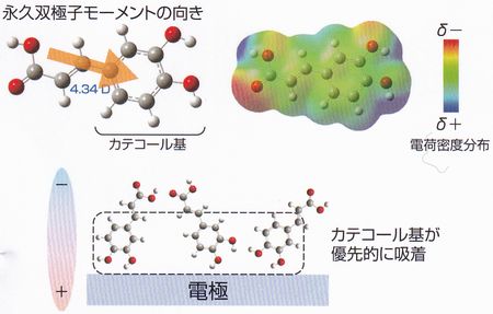
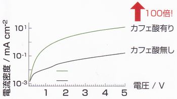
Figure 1 shows its mechanism. Molecule with dipole moment is oriented side by side by priority adsorption of catechol group include of coffeic acid on surface of electrode. As a result, work function of electrode is increased at 0.5 eV and over. In short, hole injection barrier of electrode and upper organic semiconducto is reduced, in a word, current into organic semiconductor is greatly increased. Material dependence is not almost. In fact, work function of main electrode materials, such as, Au, Ag, Cu, ITO, Al confirmed to be increased. In this experiment, a simple diode (ITO/coffeic acid/P3HT organic semiconductor/Al) was pilot produced. As figure 2�Ccurrent density was 100 times than that of device without coffeic acid.
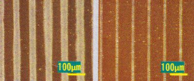
IPCE of perovskite solar cell is increased by making use of SAM as HTL As concerns perovskite solar cell, Yamagata University reported a research result of use of SAM (Self Assembled Monolayers) as hole transport layer (HTL). In this experiment, phosphonic series SAM was spin-coated on ITO electrode at 1-2 nm thickness, and then, CsPbI perovskite was spin-coated and annealed at 100 ��. The next, C60 and BCP were evaporated as electron transport layer. Finally, Al electrode was evaporated. As a result, incident photon-to-current efficiency (IPCE) of this device was increased from 18 % (reference with TFB HTL) to 20 %. This is reason why;�@Characteristics are uniformed because of enhancement of coatability of HTL in ITO surface, �AWettability of perovskite liquid is enhanced because of low contact angle (13.8 %) of surface of SAM. Emissive polymer appears as new lighting device based on triboluminescence As regards unique device and technology, Okinawa Institute of Science and Technology introduced an emissive smart polymer. It�fs an emissive device based on triboluminescence by use of frictional excitation. In short, this device is emitted by excitation of frictional heat. For example, if colored plane by highlighter pen is scrubbed, it's emitted. In this experiment, fluorescent pigment layer was covered with PVC cover film as electric device. Off course, emission color can be changed by kind of fluorescence material, and emission strength is basically proportional with fritional force. However, effective application is not found yet. Fine Cu wiring is printed by screen off-set printing As concerns printing process, AIST appealed manufacturing technology of fine Cu wiring by screen off-set printing method.
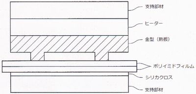
High viscosity ink can be discharged by IJ method On the other hand, Yamagata University tried to drop high viscosity ink by ink-jet printing (IJ) method. High viscosity ink same as 219 mPa�s could be stably discharged by devising operation process, for example, increase of amount of displacement of PZT by applying high voltage. As you know, low viscosity ink same as approximate 20 mPa�s should be used in IJ method heretofore. In short, inks for gravure printing and flexo printing can be used in this technology. In this research, 6 nozzles could be stably dropped. Two PI films is adhered by simple annealing Okayama University proposed new technology about direct adhesion of polyimide (PI) film and PI film without pre-treatment in the booth of New Energy and Industrial Technology Development Organization (NEDO). As you know, PI film is easily carbonized before melting because thermal decomposition temperature is greatly near melting temperature. For this reason, in case of adhering PI film, before adhesion, surface plasma is treated, or adhesive is used in the past.
Transparent organic and inorganic hybrid glass is useful for light encapsulation Ishizuka Glass appealed an original organic and inorganic hybrid glass. Its main component is SiO. It's relatively high viscosity ink before cure, but it becomes to be flexible and transparent glass-like compact after annealing at 200�� for 2h. High transmittance same as approximate 90 % in wide range (UV, NR, and IR) is obtained. Furthermore, heat resistance is high same as 300 �� order. Flexible property can be adjusted by composition.
|
||||||||||||||||||||||||||||||||||||||
| REMARK STELLA NEWS SITE is a free news site of FPD and PCB by Stella Corporation Inc.(This company does not release these FPD and PCB related products.) |
|