|
STELLA NEWS SITE is managed by Stella Corporation Inc. |

CEATEC 2023 (October 17 - 20) |
||||||||||||||||||||||||||
October 17 - 20, CEATEC 2023 were held in Makuhari Messe. Main topics of
electronics field are closed up in this here.
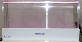
In the booth, 20.8-inch panel (1280 × 720 pixel) and 12.3-inch panel (1440 × 540 pixel) were exhibited. It showed to be suitable for face-to-face communication such as shopfront. E Ink exhibited a flexible e-paper by IGZO-TFT driving for the first time
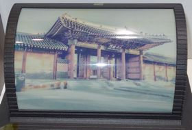
The company exhibited 8-inch color panel with glass substrate and monochrome panel (1920 × 1440 pixel) as IGZO-TFT driving panel, too. IGZO-TFT will be adopted instead of a-Si TFT in required relative speed applications. Micro-LED chip is directly patterned and mounted on the substrate by laser transfer method
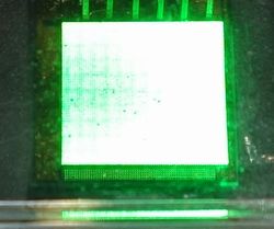
In this project, Toray and Toray Engineering developed laser transfer technology as patterning and mounting method of Micro-LED from an original sapphire substrate with LED to a display substrate by direct laser irradiation. The project pilot-manufactured a small green device with 20 × 30 dot array at 150 μm pitch. Laser transfer speed is 10,000 pieces/sec. By the way, main subject of this project is to develop advanced mounting process technology of next generation semiconductor. Micro-LED is used as device of VR/AR/MR display
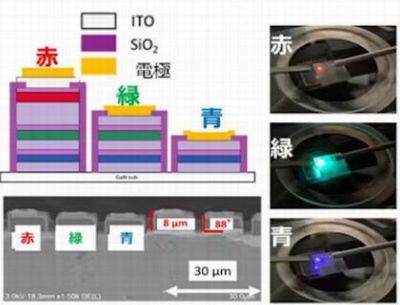
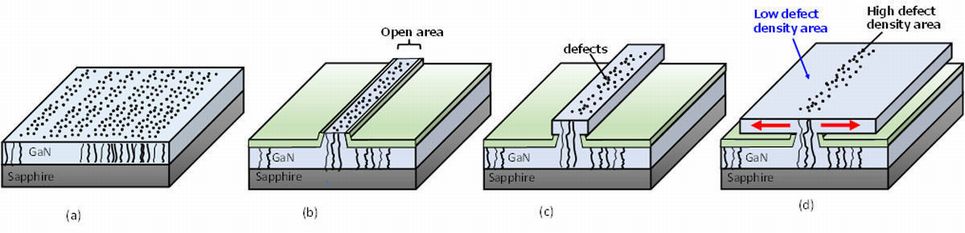
Figure 1, monolithic type full-color μLED array has been manufactured on identic substrate by stack of RGB-LEDs through of the intermediary of tunnel junction. 3 primitive color emissions of RGB were obtained. And also, a full-color display with 35 × 15 μm dot array and 330ppi resolution was pilot-manufactured. In the booth, looking and listening demonstration of head mount display (HMD) using this device was done. In this demonstration, viewer can view virtual image with 4K high resolution and large size. Docent appealed that luminance efficiency of this device was greatly higher than that of the existing OLED. Micro-LED is manufactured on a newly revolutionary substrate As concerns material for Micro-LED, Kyocera announced a newly revolutionary substrate "EGOS(ELO GaN on Sapphire)". If this substrate is used as an original substrate of LED device, LED can be manufactured in region with defect-free. Figure 2 shows process image. As (a), enormous defects of GaN is generated on grown sapphire substrate. And then, as (b) and (c), GaN is grown vertically from opening area of masking layer, as a result, growth core is generated. In this region, enormous defects exist yet. The next, as (d), crystal of GaN is grown from growth core laterally (ELO:Epitaxial Lateral Overgrowth). In this region, layer with defect-free can be formed. Device area and opening area are used as this region and general defect region respectively. As a result, high quality LED can be manufactured.
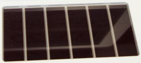
The company will supply EGOS substrate, and also, license out manufacturing technology of Micro-LED using EGOS substrate. Perovskite solar cell is built in window of high building As opening sentence, organic series solar cells have competed as a next generation device. First of all, Panasonic appealed an effective demonstration of perovskite solar cell. Main product is an integrated glass window and perovskite solar cell, and then, suitable for high building because of impossibility of setting on roof in Japanese law.
GSI Creos releases a semiconductor polymer ink, is mainly composed of Brilliant Matters's polymer
This polymer has a non-fullerene series accepter, and is bulk-hetero junction type. IPCE at champion data is 17 % because of high light absorption and low energy loss in charge process. Furthermore, in mass-production model, IPCE and lifetime are 7 % and 10 years respectively. GSI Creos supplies various inks for various coating methods, such as spin-coating, dye-coating, and so on. In the booth, device samples of Brilliant Matters and Yamagata University were exhibited. Sharp appealed dye-sensitized solar cells with high IPCE same as 20 %
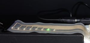
Stretchable silicon + Ag ink is suitable for wearable applications
Picture 8 shows printed sample of DuraQ on silicon rubber substrate. As you see, LED can be normally emitted. It's suitable for wearable applications, and can be sewn on clothes and has resistance against wash. |
||||||||||||||||||||||||||
| REMARK STELLA NEWS SITE is a free news site of FPD and PCB by Stella Corporation Inc.(This company does not release these FPD and PCB related products.) |
| Situation of benchmark test We are testing various treatments in respective lacations by using customer's sample substrate always. Situation of benchmark test is this page. |