|
STELLA NEWS SITE is managed by Stella Corporation Inc. |

The Total Solution Exhibition for Electronic Equipment 2023 (May 31 - June 2) |
|||||||||||||||||||||||||||||||||||||||||||||||||||||||||||||||||||||||||||||||
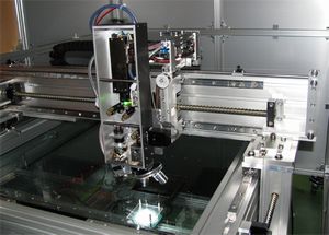
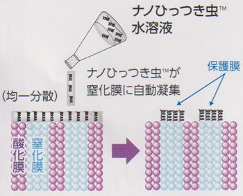
May 31 - June 2, The Total Solution Exhibition for Electronic Equipment 2023 was held in Tokyo Big Sight. Main topics of display category are picked up. Manufacturing process is simplified by selective adhesion process using new material, is adhered to nitride film onlyIn this time, most impressive product was considered to be a water solution include of secret Nano component, which was exhibited by Daicel.
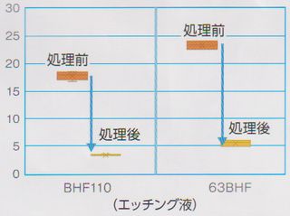
In the experiment, if this solution is coated on SiOx film, it's not adhered to SiOx film, as a result, its wet-etching ratio was not changed. On the other hand, as figure 2, wet-etching ratio of SiNx film was greatly decreased by 1/4 - 1/5 compared to reference (without coating). For this reason, in case of layer structure of figure 1, SiOx film can be etched without photoresist process-free by coating this solution only. As a result, total manufacturing process cost can be greatly reduced. Furthermore, it’s possible to thin nitride film and enlarge process margin in nitride film etching process as small merits, too. New values are obtained by fine concavity and convexity fabrication of glass surface
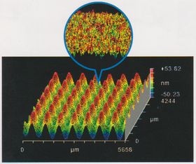
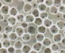
Its applications are very superior. In the booth, three applications were proposed. First application is a touch-panel. If this glass is used as a substrate, wring feeling of pen output is changed. Concretely, writing slipping is reduced, as a result, writing feeling becomes to be almost same as that of writing on a paper. Of course, it's not only pen output but also finger output. Second application is effect of enhanced adhesion. Picture 1 shows its demonstrated sample. Third effects is enhancement of hydrophobic property. Its contact angle is enlarged from 30 - 70°to 110°. Printing resolution is enhanced by use of porous PI film
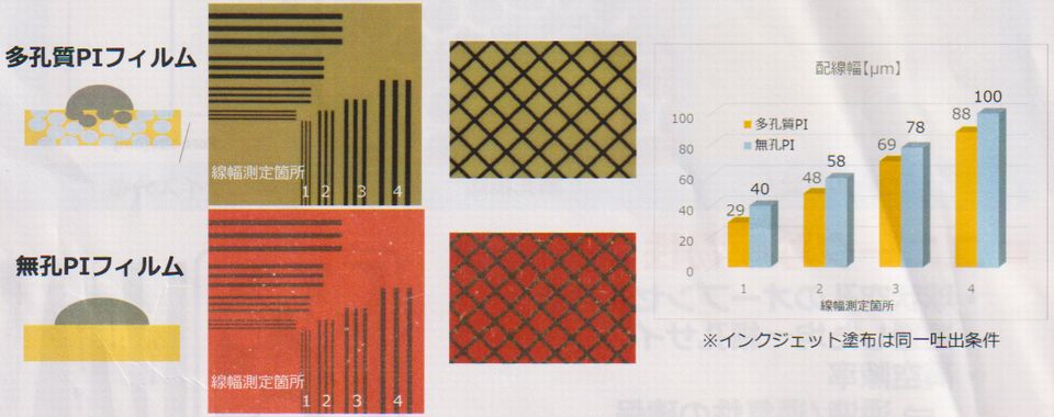
In this time, this PI film was confirmed to be effective for enhancement of printing resolution. Figure 4 shows result of Ink-Jet (IJ) printing using a metal ink. In case of using this PI film, printing resolution was greatly enhanced compared to that of using flat PI film. Of course, this is reason why printing bleeding is suppressed because of penetration of ink into fine hole. For this reason, it's effective for not only enhancement of printing resolution, but also, unnecessity of surface modification, such as insert of buffer layer, hydrophobic or hydrophilic treatment of surface, and etc. By the way, basic characteristics such as thermal resistance and solvent resistance are almost same as that of the conventional PI film, however, mechanical strength same as tensile strength is low because of its structure.
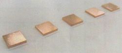
Nano Cu paste for spray coating is developed
Anneal time is greatly reduced by NIR As regards manufacturing system, Yamagata University and Komori Corporation suggested a breakthrough anneal system. It's possible to anneal Nano Ag paste for mere 1.5 - 4.5 min by use of NIR with 780 - 100 nm wavelength. Anneal time can be greatly reduced compared to the conventional oven system (30 - 60 min). NIR is absorbed into metal, however, is not absorbed into a plastic film because of its irradiation mechanism. In short, thermal damage against plastic substrate is not generated. As table 1, film characteristic for example specific resistance are almost same as that of case of using oven system. It's suitable not only Nano Ag paste and ink, but also, Nano Cu paste and solder resist ink, too. In the booth, film samples with 7 layers inclusive Ag wiring and organic insulation films were exhibited. This method was indicated to be optimum for plastic film device. By the way, NIR anneal system will be released by Komori Corporation in the near future.
|
|||||||||||||||||||||||||||||||||||||||||||||||||||||||||||||||||||||||||||||||
| REMARK STELLA NEWS SITE is a free news site of FPD and PCB by Stella Corporation Inc.(This company does not release these FPD and PCB related products.) |
|