|
STELLA NEWS SITE is managed by Stella Corporation Inc. |

nano tech 2023 (February 1-3, 2023) |
||||||||||||||||||||||
February 1-3, 2023, nano tech 2023 was held in Tokyo Big Sight. Main topics are picked up. As concerns electronics device, Ise Chemicals and Yamagata University announced to jointly develop a new quantum dot (QD) device using perovskite crystal. It's named as Perovskite Quantum Dots (PeQDs). PeQDs is a just new QD. In short, emission property is obtained by Nano size function of Nano size perovskite crystal. As you know, perovskite crystal is composed of ABX3 structure. In this material, organic cation such as MA+, transition element ion such as Pb2+, Sn2+, and halogen ion such as Br-, Cl-, I- are used as A site, B site, and X site respectively.
This PeQDs are emitted by absorption of UV light. Its photo luminescence quantum yield (PLQY) of RGB colors are 100 %. And also, in same as the conventional QD, sharp spectrum can be obtained by narrow half maximum full-width (20 - 45 nm). In the present moment, it's coated by various coating methods, but can be printed in the near future by the ink-jet printing method.
In case of the latter, G dot and R dot are patterned by use of PeQDs, on the other hand, B dot is not patterned (blank). As a result, B light of B-LED is transmitted in front without change, on the other hand, it's converted to G and R colors in G and R sub-pixels. In short, device is composed of B-LED backlight, LC cell, and PeQDs-CF. Ise Chemical is supplying a PeQDs dispersion liquid as sample in the present moment. And also, the company developed mass siesizerd method, which was named as FTFR (Forced Thin Film Micro-reactor). As a result, it's possible to mass-produce at 5000 mL/h. Really wearable OLED lighting device is realized by builting in ultra-slim battery
In this time, an ultra-slim lithium ion battery cell "EnerCera (NGK Insulators)" was mounted on reverse side of OLED module due to realization of wearable property. As a result, total thickness was reduced same as 0.55 ćo. In a word, it can be worn easily. By the way, the company will construct mass production structure by the end of the year, and released at 2024. Contact angle is increased and slit drop property is control by ultra-hydrophobic technology With respect to manufacturing infrastructure, Citizen Watch appealed an original ultra-hydrophobic treatment technology. As figure 2, polydimethylsiloxane (PDMS) is treated to ultra-hydrophobic state by fine structure using patterned laser irradiation and nanoimprinting. Typical contact angle of water is increased to approximate 150 degree.
By the way, main applications are considered to be micro flow channel, precious mold, medical systems, and so on. Structure of perovskite solar cell is simplified by use of CNT sheet as anode As regards manufacturing process of perovskite solar cell, Zeon proposed that a single wall carbon nano tube (CNT) sheet was used as anode. As figure 4, CNT sheet is directly laminated on perovskite layer as anode. As a result, device structure can be simplified by unnecessary of hole transport layer and evaporated anode. For this reason, manufacturing process cost can be reduced, too. Furthermore, corrosion does not occur because of resolution-free of halogen element. IPCE (incident photon-to-current efficiency) of the latest device is 18 % at interior, and 11 % at outdoor environment. In short, it is lower than that of the conventional device. For this reason, carrier injection height of perovskite layer and CNT sheet should be reduced in practical use. By the way, it's necessary to form a gas barrier film on CNT layer because of porous property of CNT.
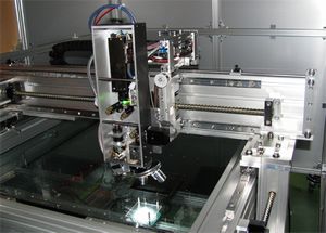
Clay material is swept and coated as gas barrier film As concerns gas barrier film of organic device, Kunimine Industries appealed a clay gas barrier material "Kunipia-RC series", which was produced at outsourcing from National Institute of Advanced Industrial Science and Technology (AIST). It's a paste inclusive of main clay composition at 20 - 60 % concentration. It's solved into acetonitrile, ethanol, and 2-propanol, and then, coated on the substrate and dried at 100 üÄ. In this coating process, montmorillonite crystals with plate shape crystal are selectively oriented by sweeping coating such as cast coating method and slit coating method. As figure 4, impurities such as H2O and O2 are blocked by stack of this clay crystal. However, water-vapor transmission ratio (WVTR) is approximate 10-2g/m2/day, which is insufficient for organic device. For this reason, it's necessary to stack this film and inorganic film such as SiN series film.
Film with ultra-high gas barrier film is useful for perovskite solar cell Toray announced to develop a barrier film with ultra-high gas barrier film, which was evaporated, for perovskite solar cell, various sensors, and so on. In this film, some inorganic compounds are co-evaporated. Its manufacturing cost is 1/5 than that of the conventional sputtering coated film because of ultra-high speed deposition and R2 process.
Polythiophene series polymer is used for conductive material and paint of flexible product
In the booth, tray for prevention of static charge, transparent heater, and film for liquid crystal shutter using this material were exhibited. It was indicated to be adopted for mass use yet. |
||||||||||||||||||||||


| REMARK STELLA NEWS SITE is a free news site of FPD and PCB by Stella Corporation Inc.(This company does not release these FPD and PCB related products.) |
|