|
STELLA NEWS SITE is managed by Stella Corporation Inc. |

FINETECH JAPAN 2022/13th FILMTECH JAPAN/11th PLASTIC JAPAN (December 7-9) |
|||||||||||||||||
December 7-9, FINETECH JAPAN 2022/13th FILMTECH JAPAN/11th PLASTIC JAPAN
were held in Makuhari Messe. Main topics in these exhibitions are picked
up.
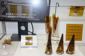
As picture 1, 15.6-inch module was exhibited in the booth. It's been mass-produced yet for notebook PC. Toppan appealed fully flexible IGZO-TFT
As picture 2, various flexible samples were exhibited. Furthermore, in the video presentation, this TFT was curved at 90üŗ, and it's pressed. Its superior flexibility was emphasized a whole lot. AIST proposed transparent heater and perovskite solar cell were manufactured by use of a new transparent conductive film As concerns material, National Institute of Advanced Industrial Science and Technology (AIST) proposed a new transparent conductive film as post-ITO film, and its effectivity for transparent heater, perovskite solar cell, and so on.
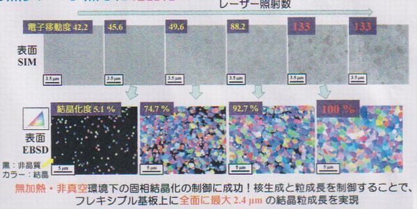
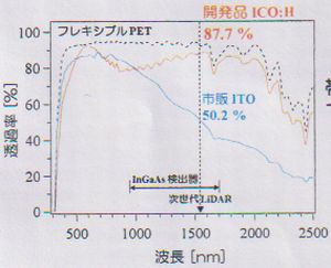
Figure 1 shows surface state of transparent conductive film and its carrier mobility. Grain size was enlarged in proportion as shot times of laser because of proceeding of poly crystal. At poly crystal state = 100 %, grain size was 2.4 ā╩m, and carrier mobility was 133 cm2/Vs. And also, typical sheet resistance was approximate 14āČ/üĀ, which is lower than that of ITO film.
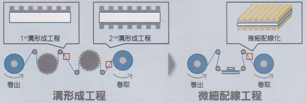
As above, it's effective for tandem type perovskite solar cell. As you know, the existing perovskite material for example CH3NH3PbX3 absorbs visible light basically, not IR light. Therefore, if a tandem device using this film as another generation unit are manufactured, highly efficient device is expected to be obtained because of high light absorption at wide wavelength range. Fine pattern with high aspect ratio can be formed by use of new metal mesh wiring On the other hand, Panasonic exhibited a both plane wiring mesh film "FineX", which was started to be mass-produced for touch sensor recently. It's a transparent conductive film with wiring mesh at both plane of plastic film, such as PET, PC (polycarbonate), and COP (cyclo-olefin polymer). It can be finely patterned and at high aspect ratio (relationship of width and thickness). Concretely, aspect ratio of the conventional etching product is about 0.25, on the other hand, that of FineX is about 0.74. In short, low resistance and high transmittance are obtained easily. Theis characteristics were realized by originally developed Roll-to-Roll process. Figure 3 shows its process image. First of all, deep ditch patterns are formed on the both plane of plastic film by the nanoimprinting method. As a result, reverse pattern against practical electrode is formed. And then, adhesive layer, Cu film, and protect layer are continuously deposited at pattern-free by wet coating method and dry coating method. As a result, a transparent conductive electrode with high aspect ratio is completed.
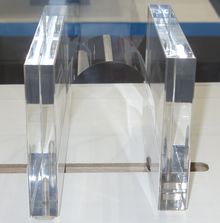
In the booth, not only simple film, but also applications were exhibited. As picture 4, it's indicated to be suitable for headup display. NEG appealed a ultra-thin glass as cover glass of foldable products
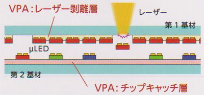
New photosentive adhesive is best suited for RGB patterning process of Micro/mini-LED Related on photosensitive material, NIPPON Chemical & Material proposed a negative type photosensitive adhesive "VPA", and appealed its unique feature. It's exposed at 100 - 500 mJ/cm2. After curing, high adhesion strength same as 20 MPa and high transmittance same as 90 % are obtained.
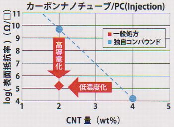
Specially effective use is RGB emission layer manufacturing process of Micro-LED and mini-LED. As figure 4, fine LED chip is transferred from 1st substrate to 2nd substrate (original substrate) selectively by irradiation of laser beam. In short, RGB emission layers can be speedily patterned by laser patterning of RGB layer each other. Dispersibility and conductivity of CNT compound are obtained at the same time
For this reason, the company doped an original additive, in order to form uniform network state of CNT. As a result, in CNT compound with resin, high dispersibility and conductivity were realized. Figure 5 shows comparison of conductive property. If this technology is used, sheet resistance becomes to be low at small content of CNT. By the way, the company does not license out, but produced CNT compound itself. |
|||||||||||||||||

| REMARK STELLA NEWS SITE is a free news site of FPD and PCB by Stella Corporation Inc.(This company does not release these FPD and PCB related products.) |
| Situation of benchmark test We are testing various treatments in respective lacations by using customer's sample substrate always. Situation of benchmark test is this page. |