NEPCON JAPAN 2019/36th ELECTROTEST JAPAN/20th IC & Sensor Packaging
Technology EXPO/20th ELECTRONIC COMPONENTS & MATERIALS EXPO/PWB EXPO/20th
Printed Wiring Boards Expo/9th FINE PROCESS TECHNOLOGY EXPO
New proposals in substrate with metal film were easy to notice
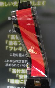
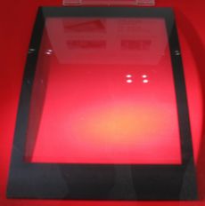
Picture 1. Demonstration of flexible OLED |
January 16-18, NEPCON JAPAN 2019/36th ELECTROTEST JAPAN/20th IC & Sensor
Packaging Technology EXPO/20th ELECTRONIC COMPONENTS & MATERIALS EXPO/PWB
EXPO/20th Printed Wiring Boards Expo/9th FINE PROCESS TECHNOLOGY EXPO were
held in Tokyo Big Site. In this here, main topics are picked up.
Yamagata University demonstrated a full flexible OLED
As concerns device, Yamagata University exhibited several OLEDs for lighting device, and appealed its superiority. Main exhibition was a full-flexible device. As picture 1, it can be bended not only vertically but also horizontally. It was encapsulated by 2 PEN films (0.1 ćo thickness), and was covered with a desiccant film on whole area of device. By the way, there were a lot of dark spot defects in this sample.
Possible to use a polymer instead of ITO as an anode by use of Al electrode mesh
As regards material, demonstrations of film with metal electrode were easy
to notice in this time. First of all, Toyo Aluminum appealed an Al mesh
electrode for OLED lighting device and organic solar cell. Figure 1 shows
its structure. Firstly, an Al foil is patterned by the wet-etching process,
as a result, Al mesh is formed. It is implanted into resin layer by an
original process.
Its surface flatness is Ra = 10 nm class, and low sheet resistance same
as 1 āČ/üĀ and under is obtained. Therefore, if it's used as auxiliary electrode
of anode, a conductive polymer such as PEDOT/PSS instead of ITO can be
used as anode. Furthermore, it's possible to form main mesh electrode and
connecting wiring in circuit of device at the same time. In this case,
it may be possible to directly connect Al electrode and IC chip without
ACF (Anisotropic Conductive Film). Of course, a device can become to be
easily flexible by making use of a plastic film substrate because of existence
of thin Al film.
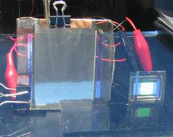
Picture 2. OLED with Al mesh electrode |
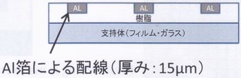 |
| Figure 1. Structure of Al mesh electrode |
The company will supply this 3 layers film. In the booth, as picture 2, an OLED lighting device was exhibited. It was pilot-produced by Yamagata University. In this sample, PEDO/PSS was used as an anode. By the way, its sales price is expected to be inexpensive compared to that of the conventional film with ITO.
Ag Nano wire film with high stability has been developed
ü@
By contrast, Showa Denko exhibited a transparent conductive film with high weather resistance and light resistance for touch-panel of in-vehicle system. In this film, an original Ag Nanosize wire is used as main component. Its sheet resistance is 35 - 40 āČ/üĀ, optical transmittance is 90 %, and haze is 0.9 %. In short, basic specification is almost same as that of the competing product.
Picture 3. Ag Nano wire transparent conductive film |
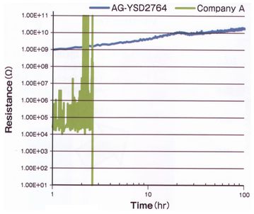 |
| Figure 2. Stability in high-temperature and high-humidity environment |
On the other hand, its durability is expected to be superior compared to that of the competing product because of using original resins, which were doped as a binder of conductive layer and overcoat layer. Figure 2 shows stability in high-temperature and high-humidity environment (85 üÄ/85 üōRH). Sheet resistance of this conductive film was not almost increased, on the other hand, that of competing reference was greatly increased. By the way, Ag layer can be patterned by the conventional manufacturing processes such as the photolithography + wet-etching method or the laser direct etching method.
Ultra-flat film can be deposited by use of a novel sputtering
With respect to manufacturing system, Canon Anelva appealed a new sputtering
deposition, which is called as the energy treatment sputtering method.
It's useful for ultra-flatness application, for example, interlayer of
semiconductor, anode of OLED, and so on. In this method, a functional film
is deposited by the sputtering method and a certain assist treatment, such
as ion implantation. In short, deposited film grows not at column shape
but at film shape. In other words, deposition is done at suppression of
grain grow. In fact, SiO2 film was deposited at 700 nm thickness on Al film (200 nm), as a result,
flatness of deposited film using this method was Ra üü 0.24 nm, on the other
hand, that of deposited film using conventional sputtering method was Ra
üü 3.73 nm. Furthermore, if film became to be thicker, there are not almost
crucks in film.
By the way, deposition ratio is lower than that of the conventional sputtering method. However, deposition process is devised, for example, firstly a film is deposited for boundary of under layer by strong assist treatment condition, and then, it is deposited by weak assist treatment condition, decrease of deposition ratio can be minimized.
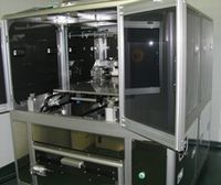
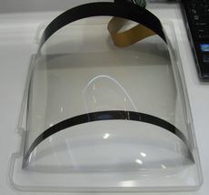
The screen printing can be adopted to curved shape
Picture 4. Printing sample on curved structure |
Micro-tec announced to release a screen printing system for curved substrate
ügMTV-850süh. It has processed stage and R guide at concave or convex shape.
It's possible to print continuously at same attack angle (for example 75üŗ)
every time. For this reason, high uniform thickness is obtained same as
that of flat screen printing process. Picture 4 shows a printed sample
on plastic film for in-vehicle application. |