28th FINETECH JAPAN Infrastructures for flexible device became to be a
major player
December 5-7, 28th FINETECH JAPAN were held in Makuhari Messe. Main topics
in these exhibitions are picked up.
JOLED exhibited various OLEDs with high quality
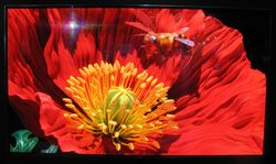
Picture 2. 54.6-inch 4K OLED (JOLED) |
 Picture 1. 21.6-inch OLED (JOLED) Picture 1. 21.6-inch OLED (JOLED) |
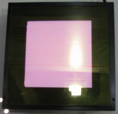
In this time, Japan Display/JOLED and Sharp attended as a display module maker. JOLED exhibited various OLEDs with high quality. Main product is 21.6-inch panel (4K panel and full HD panel), which has been released from December 2017. It's especially suitable for e-sports monitor because of high speed response (0.1ms and under).
On the other hand, as prototypes, 54.6-inch 4K panel, 27-inch 4K panel, 21.6-inch flexible panel with rotary shape structure, and 12.3-inch/12.2-inch panels for automotive system were disclosed. 54.6-inch panel is driven by oxide-TFT, by contrast, other panels are driven by LTPS-TFT. And, in all panel, top emission structure and RGB side-by-side color method by the ink-jet printing process were adopted.
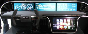
Picture 3. Display for automotive system (JOLED) |
By the way, as concerns automotive display, rigid type 12.3-inch HD panel (3 sheets) were built in main cockpit area, on the other hand, flexible 12.2-inch HD panel were built in under area.
Sharp demonstrated ultra-low reflection TFT-LCD
Sharp has demonstrated a 3-inch ultra-low reflection TFT-LCD as a prototype.
However, detail technology was not disclosed at all.
As picture 4, this panel and the conventional panel were exhibited in comparison. Its reflection ratio is 1 % and under with surface treatment film, for example anti-reflection film. By the way, reflection ratio of the conventional panel is 1 - 1.5 %. This difference is numerically mere; however, it is much in appearance for human eye.
OLED without CF is gained by use of Cd-free QD
As respect to material for display, DIC introduced a Cd-fee quantum dot (QD) ink for the ink-jet printing method. Thermal cure type and UV cure are developed. Its useful for TFT-LCD, OLED, ��-LED, and so on. It's especially effective for OLED as alternative of white EL + micro color filter (CF) panel, which has been released for large size TV recently. Concretely, if this QD is used as color changing layer with each other sub-pixel, CF becomes to be unnecessary. For this reason, loss of light transmittance becomes to disappear by CF, as a result, luminous efficiency of OLED is enhanced. As picture 5, white emission panel (structure�Ffigure 1) was demonstrated in the booth.
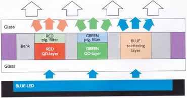
Figure 1. Structure of white emission panel using Cd-free QD
|
Picture 5. White emission panel using Cd-free QD |
DIC appealed a p-type organic semiconductor�gDOSC series�hfor organic-TFT,
too. This composition is not disclosed. High solubility type can be solved
into aromatic system solvent, chlorine solvent, and it is coated and printed
by the conventional methods, such as the spin-coating, the slit-coating,
the ink-jet printing, and so on. In spite of wet-coating type, relatively
high carrier mobility same as 2 cm2/Vs is obtained. On the other hand, high carrier mobility type is deposited
by the evaporation method due to low solubility. However, its carrier mobility
is high same as 10 cm2/Vs. Its means that this value is almost equal to that of oxide-TFT. By
the way, both types have superior atmospheric stability.
Flexible substrate with inexpensive glass paste was introduced
Picture 6. Stacking plate of glass and SUS |
Toyo Kohan introduced a unique flexible substrate, which is composed of SUS base substrate, surface modification layer, and thin film glass layer. Of course, SUS has flexible property, and glass layer has flat surface, insulation, and gas barrier properties. Glass film is formed by coating or printing a low melting point glass paste and firing at 400 - 500 ��. As a result, flat surface is obtained same as Ra �� 0.4 nm�ARz �� 4.8 nm. As you can image easily, its total cost is drastically low compared to that of standard structure (for example, PI film + vacuum deposited organic and inorganic hybrid films). For this reason, it's suitable for flexible OLED and flexible organic solar cell.
Transparent electrode and auxiliary electrode are formed on flexible roll glass
By contrast, Nippon Electric Glass (NEG) demonstrated a flexible glass with roll shape �gG-Leaf�h in this time extensively. Green OLED lighting device (made by Yamagata University) using G-Leaf were exhibited. This device was encapsulated by G-Leaf as another encapsulation substrate, too. It demonstrated that G-Leaf was effective for an encapsulation substrate.
Picture 7. Transparent electrode and auxiliary electrode on the G-Leaf
|
Furthermore, NEG exhibited a 800 �o width sample roll with IZO transparent electrode, insulation layer, and auxiliary electrode on G-Leaf. Auxiliary electrode was directly printed by the screen-printing method. If it is formed on transparent anode, a large OLED lighting device can be manufactured easily without ununiform brightness.
Geomatec releases a moth eye film
Geomatec developed a surface treatment film �gg.moth�h, and then, announced to enter into a new market. TAC film is directly treated by the Nano-imprinting method, as a result, moth-eye structure such as eye of moth is formed on surface of TAC film. For this reason, reflection ratio is minimized, and, light transmittance is increased. Furthermore, hydrophobic property is obtained on the surface by moth eye structure, and contact angle is increased same as 150��(water). As picture 8, various samples were demonstrated in the booth.
RT junction advanced to transparent RT junction
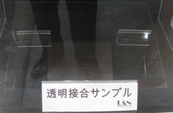
Picture 9. Transparent junction sample |
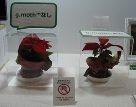
Picture 8. with g.moth (left) and without g.moth sample (right) |
As concerns manufacturing system, Lantechnical Service announced a new RT (room temperature) junction technology of various substrates. The company has succeeded RT junction of various substrates by making use of original ion beam sputtering and assemble technology in the past, and then, in this time, the company has succeeded transparent RT junction. A new material (secret) is used as junction material due to replacing Si series material. As a result, transparent RT junction was realized without change of manufacturing process. It's possible to correspond to various substrates, such as glass, silicon wafer, ceramics, PET film, PEN film, and so on. And also, it's possible to control junction strength by optimization of sputtering process and after process (pressure reduction process).
Deposition rate of FTS is enhanced by a new cathode unit
Keihin Ramtech proposed a new FTS (facing target sputtering) method using an original cathode unit (RAM cathode). It is an advanced cathode and deposition method of FTS, which is known as a low damage sputtering method. In conclusion, high deposition rate is obtained with keeping low damage property.
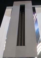
Picture 10. RAM cathode (Keihin Ramtech) |
In addition to orthogonally set 2 targets against the substrate, 2 targets are set in the top and bottom side of above targets. As a result, acceleration force of Ar ion is increased because of generation of plasma in neighborhood of target. For this reason, deposition rate becomes to be enlarged due to increase of sputtering grains, which are belted out target. In fact, deposition ratio of ITO film was 3 times than that of deposited ITO film by the conventional FTS. Utilization ratio is same as approximate 40 %, which is almost equal to that of the conventional sputtering method using shaking magnet cathode. Of course, low damage property is easily obtained same as 1/3 and under compared to that of the conventional sputtering method because of minimization of incident Ar ion against the substrate.
The company will supply this RAM cathode unit to sputtering system makers,
and, develop and release a test system for pilot-production use in the
future. |