|
STELLA NEWS SITE is managed by Stella Corporation Inc. |

Innovation Japan 2017 (August 31- September 1) |
||||||||||
August 31- September 1, Innovation Japan 2017 was held in Tokyo Big Sight. Main topics for electronics in this exhibition are picked up. Carrier injection height of OLED is reduced by new ceramic materials
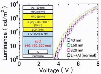
First of all, the research group (Professor. Hideo Hosono) of Tokyo Institute of Technology appealed new ceramic buffer materials for OLED. One is C12A7(12CaOź7Al2O3) electride as electron injection material in the past. In electride which is a compound, positive ion is ionically-bonded with electron instead of negative ion. C12A7 electride has Nano size ceramic with cage shape, and contains electron which functions as negative ion. Even ceramic, it has conductance and filed emission property. Work function of crystal is mere 2.4 eV, and that of thin film is approximate 3eV. Furthermore, it is easy to treat because of chemical stability. AGC is releasing the C12A7 sputtering target at the moment for sputtering deposition process. Of course, it can be deposited at room temperature by the sputtering method, and can be easily patterned by making use of the conventional acid series etchant. Another is ZSO (Zn-Si-O) buffer material. It has high transmittance against visible light and superior flatness at film state. For this reason, it's possible to form transparent electrode by stacking with metal electrode such as Al. And also, work function is mere 3.5 eV. AGC is releasing this sputtering target, too. This material can be deposited and patterned by conventional deposition and wet etching processes. In this time, the research group proposed this double layer for electron injection layers of inverted structure type top emission OLED. In short, lower carrier injection height (4.13eV (Al cathode) ü© 3.5eV (ZSO buffer layer) ü© 3eV (C12A7 HIL)) is gained by use of layer structure of figure 1. In fact, as figure 1, emission property of this test device is higher than that of reference device (inverted structure OLED with LiF/Al cathode) by optimization of thickness of ZSO film. Carrier injection height is decreased by use of a new transparent anode
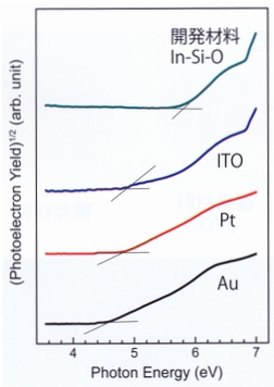
On the other hand, Kogakuin University proposed In-Si-O as a new transparent anode material for OLED. As figure 2, it has high work function same as 5.0 eV and over at as-depo state by optimization of dopant ratio. If it is used as transparent anode instead of conventional ITO, carrier injection height is decreased without surface treatment after deposition. And also, surface flatness is superior same as rmsüü0.2nm because of amorphous structure, so thatüCit may be unnecessary to flat such as polishing or annealing after deposition. Of course, it can be deposited by the conventional sputtering method. Large size LED display is driven by OTFT
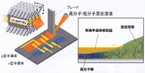
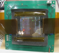
As regards organic-TFT, the research group of Tokyo University (Professor. Takeya) reported the result of JST project (Development project of active matrix for large size sheet display). This research group is known as development of coating and single crystallization method of organic semiconductor. In this time, as figure 2, wettable n-type and p-type organic semiconductors are singly crystalized by sweeping the blade, as a result, organic COMS circuit is formed on 100 ü~ 100 ćo substrate. On the other hand, this organic-TFT array is transferred to the display substrate with electrodes by use of adhesive; as a result, active matrix sheet is completed. RGB-LEDs are mounted to this organic-TFT array, and then, the completed 100 ü~ 100 ćo devices are mounted to 500 ü~ 500 ćo sheet. By use of PEN films as both substrate, light weight (2 kg), thin body (3 ćo), andü@flexible (Rüü10 cm) display is gained. It is expected to be used as various applications, such as large size display for indoor, poster, banner, and so on.
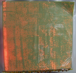
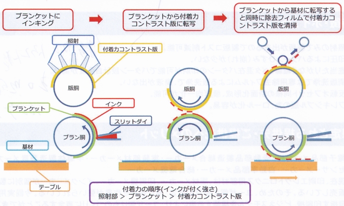
Picture 1 shows a sample device. It does not emit at whole plane because of incompletion of manufacturing process, however, it is varied that LEDs can be driven by organic-TFT. New printing technologies disappear on the scene With relation to manufacturing process of devices, in this time, new printing technologies grabbed the spotlight. Firstly, the research group of University of Hyogo and Asahi Kasei reported R2R (Roll to Roll) Nano size patterning technology as the result of JST project. In this R2R printing technology, etched gravure cylinder by electron beam exposure technology is used as a printing mask. Detail mechanism is not disclosed because of group's know-how, however, ultra-fine line same as 250 nm can be directly printed. In this time, transparent electrode grid was exhibited. In this sample, Cu ink was printed at line width 1 ā╩m as matrix pattern. As picture 3, LED could be emitted by this invisible transparent wiring. Mask is directly formed at in-situ, and then, it's used as printing mask Nihon Denshi Seiki which is a printing system maker announced a new printing technology without mask, which was developed by NEDO project. It is named as adhesion contrast printing. In this method, difference of adhesion of ink is skillfully applied.
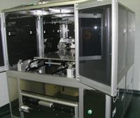
Concretely, as figure 4, first of all, laser beam is irradiated to adhesion contrast mask at pattern shape by the laser direct exposure method and etc. As a result, ink adhesion in irradiated area is increased, that in nonirradiated area keeps initial week adhesion. By contrast, an ink is coated to silicon blanket roll by the slit die coating. The next, mask roll and blanket roll are contacted, so that, unnecessary ink is transferred from blanket roll to mask roll. And then, patterned ink is transferred from blanket roll to the work substrate. As the above, ink adhesion is expressed that irradiated area üä blanket üä adhesion contrast mask. By making use of this phenomenon, ink is patterned. By the way, after transcription, adhesion contrast mask is cleaned by use of eliminated film. And then, the next substrate is printed. Printing resolution of this method is minimum 2 ā╩m. After 100 times printing, repeatability of pattern is not almost changed. Firstly, a test machine for 200 ü~ 200 ćo substrate was developed. Tact-time of this machine is 90 sec. And also, alignment accuracy is 1 üō and under. However, there is not a laser irradiation unit in this test machine, so that, user have to prepare a laser irradiation system or unit afresh. |
||||||||||
| REMARK STELLA NEWS SITE is a free news site of FPD and PCB by Stella Corporation Inc.(This company does not release these FPD and PCB related products.) |
Novel system was released as manufacturing system of emulsion film mask. |