|
STELLA NEWS SITE is managed by Stella Corporation Inc. |

JPCA Show 2017 (June 7-9) |
|||||||||||
June 7-9, JPCA Show 2017 was held in Tokyo Big Sight. Main topics in these exhibitions are picked up.
First of all, in regard to plating process, Tanaka Kikinzoku Kogyo introduced an original process, which is developed by Electroplating Engineers of Japan, subsidiary of Tanaka. In this process, firstly, an original photosensitive primer is coated on the substrate such as PET film, glass, and then, it is exposed by UV exposure. The next, the substrate is dipped into colloid catalyst liquid inclusive of Au Nano size grain catalyst and then, it is dipped into various electroless plating solutions, which are inclusive of metal catalyst. As a result, fine pattern is formed on the substrate. In this process, acceptor exists on the surface of primer layer. It is patterned by UV exposure using 300 nm wavelength. Therefore, Au Nano size grain catalyst is absorbs to area with acceptor selectively. By the way, acceptor only is eliminated by exposure; on the other hand, primer layer remains at without patterning state as under layer. As you can image easily, process temperature is low such as 100걥 and under. And also, low resistance wiring is gained, for example, 3.3 꺤꺐cm (Au), 2.3 꺤꺐cm (Cu). Tanaka exhibited various samples (substrate갌glass, PET film, polyimide film, metal film갌Au, Cu, Ni, Pd) on the booth. In short, this process can be corresponded to various substrates and metal kinds. Cu film is directly plated on the resin substrate by use of plasma surface treatment On the other hand, Osaka Research Institute of Industrial Science and Technology proposed a new plating process using plasma surface treatment technology.
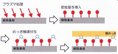
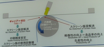
As figure 1, a plastic film such as fluorine resin substrate, polyimide substrate is treated by vacuum plasma treatment; as a result, functional group on surface of the substrate is eliminated. The next, other functional group is formed on the substrate by purging reactive gas such as fluorine series gas. Subsequently, plating catalyst is adhered to the functional group selectively, and then, Cu film is plated by self-aligned mechanism. In short, it's possible to plate Cu film on the substrate directly. Of course, in the past, this direct plating was considered to be impossible. Plasma treatment, dipping, and plating processes are done in the low temperature environment, so that; this process is effective for flexible device. And also, if the substrate is exposed by UV exposure after introduction of other functional group, Cu wiring can be formed easily. By the way, adhesion of Cu film against the substrate is estimated to be 0.7kN/m (peel strength). This value is superior to that (0.6kN/m) for required FPC. For this reason, this process is effective for high-frequency circuit (fluorine resin substrate) and flexible device (PI substrate) because of low temperature process. Distortion of screen mask is resolved by use of new printing technology
Seria Corporation appealed a new screen printing process for plastic film substrate. Figure 2, in this process, while a film substrate is transferred by the rotary cylinder and a metal paste is printed at 0 clearance (printing gap). Rotary screen printing is printed at 0 clearance by use of rotary screen mask, on the other hand, this new process is printed by use of conventional flat screen mask. Distortion of screen mask is resolved by printing mechanism, and also, fine pattern same as L&S걖30꺤m/30꺤m can be printed continuously. Printing speed is 15-20 second (@300뇇 size). In the booth, sample for OLED lighting device with printed Ag paste for anode auxiliary wiring (made by Yamagata University) was exhibited. Noritake introduce new Ag pastes As concerns electronics material, Noritake Company Limited demonstrated world highest quality Ag paste and low temperature firing Ag paste.
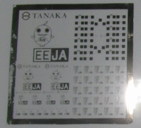
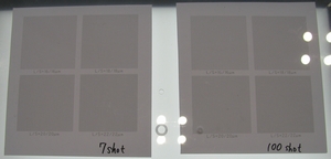
In the former, in spite of using 꺤m size Ag powder, fine pattern same as L&S걖16꺤m/16꺤m can be printed by the screen printing method. The company appealed that this resolution was world highest quality. And also, if ultra-thin film type is used, covering ratio against surface of the substrate is 100 걪 at 1.5 꺤m thickness. Density conductive film without void is gained. On the other hand, if ultra-thick film type is used, ultra-thick film same as 80 꺤m thickness can be coated. In the booth, as picture 2, 7 shots printed sample and 70 shots printed sample are exhibited in comparison. The company indicated that printed quality of the later is almost same as that of the former. In low temperature firing Ag paste, 꺤m size Ag powder is used as main component, too. In general, in this grain size, melting point drop effect is not gained갍 however, in this Ag paste, each Ag powder is perfectly contacted on the substrate by devising binder composition. Low resistance for example, 8 꺤꺐쩭m (annealing temperature갌100걥), 3.6꺤꺐쩭m (250걥) is gained. For this reason, this Ag paste can be printed on not only glass, ceramics, but also, plastic film, document paper. |
|||||||||||
| REMARK STELLA NEWS SITE is a free news site of FPD and PCB by Stella Corporation Inc.(This company does not release these FPD and PCB related products.) |
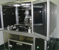
Novel system was released as manufacturing system of emulsion film mask. |