|
STELLA NEWS SITE is managed by Stella Corporation Inc. |

nano tech 2017 (February 15-17) |
|||||||||||||||||||||||||||||||||||||||||||
February 15-17, nano tech 2017 were held in Tokyo Big Sight. Main topics in this exhibitions are picked up. Display can be cut by scissors
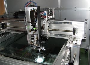
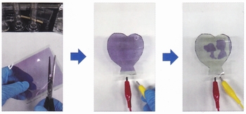
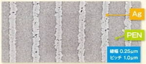
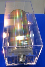
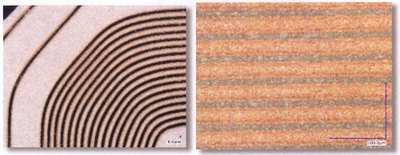
First of all, as concerns electric devices, research group of Chiba University demonstrated color electrochromic display (ECD) in the NIMS's booth. Its catchphrase is to be possible to cut at will by scissors. As its name, if this display is cut at optional shapes, it shows the image on the screen by jointing terminals to ITO transparent electrodes on the both substrates. As you can image, this means that it is difficult to degrade in the atmosphere environment, because organic-metal compound polymer and solid electrolyte are greatly insensitivity against the atmosphere. In the fact, this prototype is not encapsulated. Therefore, it's advantageous for lifetime compared to other displays such as OLED. In ECD, while a certain voltage is applied, oxidation-reduction reaction happens on the electrode, as a result, display's color changes from transparent to original color of polymer. Furthermore, if applied voltage is increased, color becomes to be transparent again. As you know, their memory characteristic is a few dozen minutes. The research group has developed cyan (Fe series), yellow (Co series), and magenta (Ru series) in the past. Not only multi-color panel but also full-color panel is realized easily by stacking this 3 layers. Career mobility of CNT-TFT was dramatically enhanced With respect to CNT-TFT, Toray exhibited a CNT-TFT array on the polyimide film in this time, too. In this device, CNT complex which is composed of single-wall CNT and P3HT conductive assisted polymer is used as an active layer, in order to enhance dispersion characteristics in liquid state. In this experiment, CNT layer was deposited and patterned at the same time by the ink-jet printing method. This device was not basically new, however; TFT property was greatly enhanced in this time. Concretely, career mobility is increased from the past value (13 cm2/Vźs) to 80 cm2/Vźs. This is reason why damage against CNT was dramatically suppressed by optimization of ultra-sonic irradiation treatment in the manufacturing process of CNT complex. As a result, it becomes to be adopted to display use. By the way, bending durability is sufficient. In fact, TFT property changes rarely in the bending state. High resolution same as semiconductor photolithography is realized by gravure printing Most impact of device manufacturing infrastructure in this exhibition was high resolution Roll to Roll printing technology by Asahi Kasei. It's a gravure printing technology using Seamless Roller Mold (SRM), which was originally developed by the company. It is manufactured by patterning photoresist by the electron beam exposure and etching surface of SRM using this photoresist masking pattern. If this technology is used, ultra-fine pattern such as line width 100 nm or under can be printed. Etching method was not disclosed due to technology know-how, but seems to be dry-etching method considering resolution. Of course, real printing resolution is extremely high, as picture 4; Ag Nano size ink could be printed at line width 250 nm, and also, could be printed as gate electrode and S/D electrode of 2000 ppi resolution for a flexible TFT. As you know, its resolution and precision are close to that of semiconductor photolithography.
The company exhibited 250 ćo and 70 ćo in width SRM in the booth. Printing speed of original gravure printing system is 8 m/min at a maximum. As concerns business style, the company will supply a plastic film with some functional films, which is printed by this printing technology; first of all, the company has developed high resolution transparent conductive film (TCF) with Ag grid electrode. Line width of this sample is 1 ā╩m, however; as the above, line width of 250 nm was confirmed in the experiment. Thus, in the case of this high resolution, really invisible transparent conductive film is gained because line with is shorter than that of light wavelength. This technology has been developed recently, so that, there are some problems for practical use for example correspondence to large size substrate. However, if technology is brushed-up at a good rate, it becomes to be large threat of the Nanoimprinting method. Printing accuracy is complemented by use of hydrophobic material
On the other hand, Nissan Chemical Industries appealed a hydrophilic/hydrophobic material as an assisted material for fine printing process. Before patterning of fucntional films by various printing methods for example the IJ method, this material is coated by various coating methods, to enhance to printing accuracy by surface treatment of the substrate, and then, it is burned at 140 üÄ, finally, it is exposed by UV light with wavelength 365 nm at 100 m/cm2. As a result, UV irradiated area changes from hydrophobic property to hydrophilic pproperty, on the other hand, non-irradiated area keeps at initial property (hydrophobic property). Table 1 shows contact angle against various solvents. As the table, contact angle changes greatly by chemical treatment using exposure porcess. After exposure, if a metal ink is directly printed or a catalyst is printed and then Ni is plated self-selectively by the non-electrolytic plating method, fine metal pattern is gained easily. By the way, exposure resolution is 5 ā╩m at a minimum. Yamagata University appeals tow low cost technologies for organic-TFT
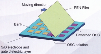
Yamagata University introduced two new processes for organic-TFT. One is a cardo type polymer, which has been developed by collaborative development with Nippon Steel & Sumikin Chemical. If this material is used as a gate insulator material, gate insulator layer and contact hole can be manufactured by 3 steps (coating, exposure, and development) due to photosensitivity. In short, process step numbers can be greatly reduced compared to that of the conventional photolithography. Insulation durability is same as that of PVP and CYTOP, which are general gate insulator material for organic-TFT. And also, device property is gained at same value as that of the conventional device with these gate insulator films. Another is a new patterning process of organic semiconductor layer (Solution Shearing). As figure 1, as preparation, bank pattern is manufactured except for channel area in advance by photolithography, and then, an organic semiconductor liquid is dropped in the center of the substrate, the next, PEN film is contacted to the substrate and moved by sweeping. As a result, organic semiconductor layer can be manufactured on channel area selectively, because it is adhered to channel area only due to existence of hydrophobic bank. It seems that orientation and increased grain size effect are expected superficially, however; these effects are confirmed yet. Thus, research group is appealing this process as a low cost process technology for a time. OLED with grafen anode is pilot-produced
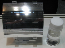
AIST appealed high speed synthesis method of grafen using plasma treatment technology, and then, exhibited an OLED device with transparent graphene anode, which was made by this method. Concretely, cupper foil substrate is treated at 1000 üÄ and over by the thermal CVD method using purged methane gas, As a result, graphene sheet is formed on the cupper foil substrate for mere 1 minute. This graphene sheet is transferred to the device substrate by making use of PMMA polymer adhesive. Picture 6 shows pilot-produced OLED device. If this device is bent, it does not degrade at keeping initial luminescent state. In short, it is confirmed to be suitable for flexible devices. However, device characteristic is not estimated inclusive of comparison of the conventional ITO anode OLED. By the way, graphene film can be patterned easily by dry-etching using O2 gas. Functional film is directly patterned by laser etching
As regards manufacturing system, Ricoh introduced laser patterning system for functional films RICOH LA-1100, which has been released from Ricoh Industrial Solutions, a Ricoh's subsidiary company. By using this system, in the case of 500 ü~600 ćo substrate, functional film can be directly patterned for approximate 1 minute due to two-dimensional scanning using galvanometer mirror. In the past, the company has been focused on ITO transparent film mainly, however, in this time, the company tried to pattern Ag and Cu ink (and paste). As picture 7, these metal films were confirmed to be fine-patterned in fact. However, it's necessary to pattern these metal films by 2 times of laser etching because of thick film. |
|||||||||||||||||||||||||||||||||||||||||||
| REMARK STELLA NEWS SITE is a free news site of FPD and PCB by Stella Corporation Inc.(This company does not release these FPD and PCB related products.) |
|