|
STELLA NEWS SITE is managed by Stella Corporation Inc. |

The 84th JSAP Autumn Meeting, 2023 (September 19 - 23) |
||||||||
September 19 - 23, The 84th JSAP Autumn Meeting, 2023 was held in Kumamotojo-jo
hall and other surrounding facilities. Topics of OLED, oxide-TFT, and perovskite
solar cell are closed up based on the proceeding.
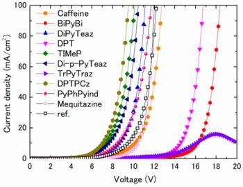
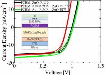
On the other hand, in case of using TIMeP and DPTPCz, driving voltage were reduced to 2V and over. Furrthermore, in the former, EQE was increased, too. By contrast, if DPTPCz was used, driving volatage was lower than that of the conventional device using LiF only EIL. ETL of perovskite solar cell is formed by meniscus and transfer method With respect to perovskite solar cell, the research group of Shinshu University announced that electron transport layer (ETL) of device was formed by meniscus method and transfer method instead of spin-coating method. A substrate with ITO film was dipped into SAM MeO-2PACz liquid, and then, it was annealed at 100 �� for 10 min due to formation of hole buffer layer. The next, perovskite precursor liquid was spin-coated. The next, in case of conventional method, PCBM liquid was spin-coated, and then, ZnO liquid was dropped, and annealed in N2 at 100 �� for 10 min. On the other hand, in case of this new method, PCBM film was coated on PDMS stamp at 3-10 nm as release layer, and then, ZnO film coated by the meniscus method, and annealed in N2 at 120 �� for 20 min. And also, PCBM film was coated on perovskite layer side by the meniscus method, and then, stamp was dipped into toluene, and then, it transferred on PCBM film by press method. Finally, Al film was evaporated.
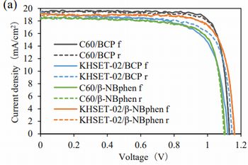
As you image easily, used amount of PCBM and ZnO can be reduced at 1/10 and under compared to that of spin-coating method. Perylenediimide precursor is useful for ET material of perovskite device instead of C60 On the other hand, the research group of AIST and Chemipro Kasei proposed to use perylenediimide (PDI) precursor as ET material of perovskite solar cell instead of C60.
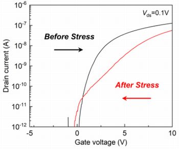
As figure 4, IPCE and Voc of the conventional device with C60/BCP were 18.3% and 1.13V respectively, on the other hand, those of inverted structure device with KHSET-02/��-NBphen were 17.4% and 1.16V respectively. In short, PDDI precursor can be used as ET material of inverted structure perovskite solar cell. Durability of negative bias stress of top-gate type IGZO-TFTs is estimated Concerns as IGZO-TFT, Nara Institute of Science and Technology reported estimated result of durability of top-gate type IGZO-TFTs, which was advantageous for high resolution and high frequency compared to the conventional back-channel type bottom-gate IGZO-TFTs.
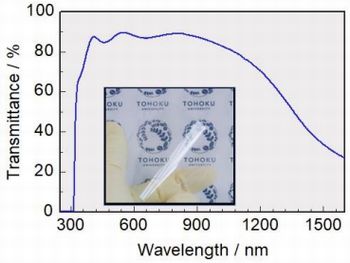
As figure 5, after NBTIS stress, Vth of this IGZO-TFT was shifted to positive direction. This degradation is considered to be caused by 3 elements, �@occurrence of hamp in low Vg region after NBTI stress, �Apositive shift of Vth against initial characteristics, �Breduction of drain current against initial characteristics. This degradation phenomenon was confirmed to be depended to device structure and shape. ITO film is deposited in atmosphere by mist deposition method As regards manufacturing process, the research group of Nikon and Tohoku University proposed to deposit ITO film in atmosphere environment by the mist deposition method. In this experiment, Nano size ITO liquid is changed to mist state (��m order grain), and transported to the substrate by carry gas. Its transporting gas fluid flow can be precisely controlled. Furthermore, Dispersed Nano size ITO grain into water has developed without addition agent. As a result, it's unnecessary to treat at high temperature. In short, low thermal resistance substrate can be used.
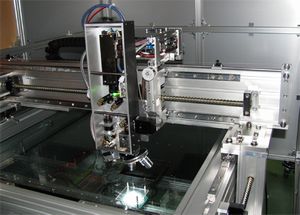
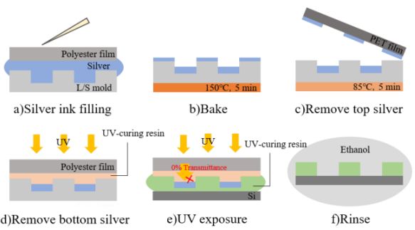
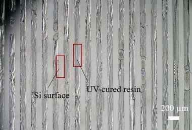
Non-residual-layer nanoimprint using Ag ink The research group of Tokyo University of Science proposed a new process as manufacturing method without residual-layer, which was generated after nanoimprinting and UV cure of UV-curing resin. Shows 7 shows process flow. First of all, Ag ink is coated on a master mold (silicon wafer) with L&S=100��m pattern by wooden pick (a), and then, annealed at 150�� for 5min by the hot plate due to deposition of Ag (b). The next, a PET film is compressed to the master mold, and then, annealed at 85�� for 5 min, as a result, it's released film due to elimination of residual Ag in bump part (c). Subsequently, UV-curing resin is filled between the master mold and polyester film due to elimination of residual Ag in ditch area. And then, it's transferred to polyester film by irradiation of UV light from upper side (d). In transferred film, Ag is adhered to bump area of pattern. For this reason, it's dipped into Optool-DSX 1% due to enhancement of release property of Ag surface. The next, UV-curing resin is filled between silicon substrate and polyester film side, as a result, polyester side is released by UV irradiation from upper side of polyester film (e). Finally, non-curing area of Ag is rinsed by ethanol (f). As a result, 100 ��m width line was patterned without residual-layer (picture 1).
Reference 1)Murai, et.al.�FElectron injection ability of nitrogen-containing heterocyclic compounds in OLEDs, The 84th JSAP Autumn Meeting, 2024, 11-497 (2023.9) 2)Koike, et.al.�FFabricated of inverted perovskite solar cells with transfer printed electron transporting layers, The 84th JSAP Autumn Meeting, 2024, 11-426 (2023.9) 3)Araki, et.al.�FInverted type perovskite solar cells with a non-fullerene electron transport material, The 84th JSAP Autumn Meeting, 2024, 11-456 (2023.9) 4)Takeda, et.al.�FDegradation Analysis under Negative Bias Stress and Light Irradiation in Top-gate In-Ga-Zn-O Thin Film Transistors, The 84th JSAP Autumn Meeting, 2024, 16-012 (2023.9) 5)Nishi, et.al.�FDeposition of High-Performance ITO Nanoparticles Utilizing Mist Deposition under Atmospheric Conditions, The 84th JSAP Autumn Meeting, 2024, 05-208 (2023.9) 6)Nakamura, et.al.�FNon-residual-layer nanoimprint using silver ink without vacuum process, The 84th JSAP Autumn Meeting, 2024, 06-034 (2023.9) |
| REMARK STELLA NEWS SITE is a free news site of FPD and PCB by Stella Corporation Inc.(This company does not release these FPD and PCB related products.) |
|