|
STELLA NEWS SITE is managed by Stella Corporation Inc. |

The 69th Japan Society of Applied Physics (JSAP) Spring Meeting 2023 (March 15-18) |
|||||||||||
March 15-18, The 70th Japan Society of Applied Physics (JSAP) Spring Meeting
2023 was held by the hybrid method (Sophia University and online). Main
topics of electric devices are closed up based on the proceeding.
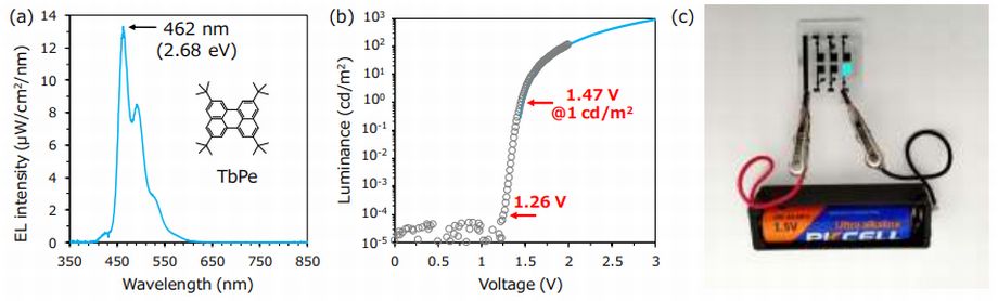
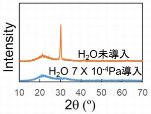
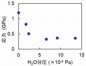
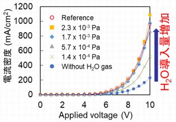
Damage against organic device is suppressed by controlling crystallinity of ITO On the other hand, National Institute of Advanced Industrial Science and Technology (AIST) reported that damage against transparent OLED could be reduced by deposition of ITO electrode at low stress. In this experiment, a top ITO electrode was deposited by the facing target sputtering method, and then, a transparent OLED was pilot-produced. In deposition process of ITO film, H2O gas was injected into the vacuum chamber at 10-4 Pa due to preventing crystallization of ITO. Figure 2 shows diffracted spectrum of X-ray. If H2O gas was injected at 10-4 Pa, ITO film was completely changed to amorphous state. Figure 3 shows relationship of stress and doping amount of H2O. If H2O gas was injected, stress was reduced from 1.25 Mpa to 0.3 MPa. And also, current-voltage characteristic was enhanced by injection of H2O. In short, characteristics of transparent OLED can be improved by controlling partial pressure of H2O in deposition process of ITO film.
Carrier mobility is increased by use of In5GaZnO10 instead of conventional InGaZnO4 With respect to oxide-TFT, Kobe University proposed In5GaZnO10 instead of conventional InGaZnO4 as oxide semiconductor, and then, succeeded to increase carrier mobility of a-IGZO-TFT greatly.
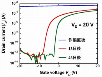
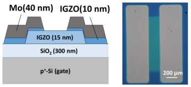
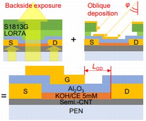
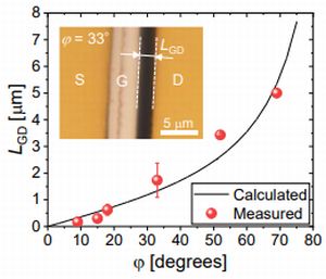
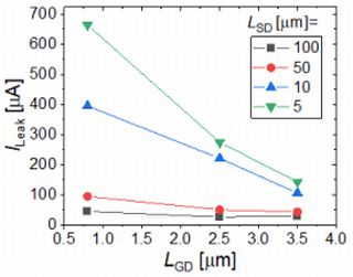
Figure 6 shows transfer characteristics. As produced IGZO-TFT, drain current is slightly modulated by gate voltage, however, it's not reduced to 10 mA and under in this voltage field. On the other hand, after 13 days and after 45 days, normal transfer curve was obtained at normally on mode. Their carrier mobility of after 13 days and after 45 days was 51.9 cm2/Vs and 40.3 cm2/Vs in saturation region respectively. This is reason why carrier density was reduced by reaction of oxygen defect of surface of In5GaZnO10 film and oxygen in air, vary with time, as a result, after 13 days and over, In5GaZnO10 film was changed to semiconductor property. For this reason, high carrier mobility was obtained than that of the conventional InGaZnO4-TFT. Leak current of CNT-TFT with plastic substrate is suppressed by asymmetric-gate structure As concerns carbon Nano tube-TFT (CNT-TFT), the research group of Nagoya University and AIST indicated that it's possible to adopt asymmetric-gate structure on a plastic substrate due to reduction of leak current. In the past, the research group has developed an original forming process of gap length of drain and gate (LGD) at self-aligning by back exposure and oblique evaporation. In this time, a CNT-TFT with symmetric-gate structure was pilot-produced on PEN film (figure 7). Channel length (LSD) was 5μm, 10μm, and 50μm, channel width was 100 μm. First of all, semiconductor type CNT was deposited, and then, Ti/Au electrode was formed as a source/drain. The next, an electron was doped into source/drain by use of KOH and crown ether (CE). Subsequently, Al2O3 film was deposited at 45 nm thickness as gate insulator. In forming process of gate electrode, the substrate was exposed from back side by the intermediately of transparent PEN substrate. In short, LGD pattern was formed by use of masking of source/drain. The next, Ti/Au gate electrode were evaporated from oblique direction (angle φ), which was 18, 33, and 52 degree. As figure 8, LGD was increased in proportion as φ. It's correspondent with advance forecast based on height of photoresist and φ. In short, it's confirmed to be possible to control LGD by φ. Fig.9 shows dependence of leak on LGD at VDS = 5 V and VGS = -5 V. Leak current was decreased in proportion as increase of LGD, and also, effect of asymmetric-gate structure was towering in case of device with short channel particularly.
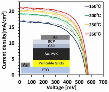
New solution-processed HTL is used for Sn series perovskite solar cell As regards perovskite solar cell, recently, candidate of Pb series device are attracted attention because of ecological feature (Pb-free). As you know, Sn series and Bi series are major candidates of Pb series device. In this time, The University of Electro-Communications reported a new transport hole material for Sn-PVK PV.
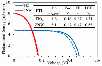
Figure 10 shows I-V characteristics of Sn-PVK PV with printable SnOx layer prepared at various annealing temperatures. Short circuit current density (Jsc) was increased in proportion as annealing temperature. In case of 350 ℃ anneal, IPCE (incident photon-to-current efficiency) was maximum same as 8.54 %. New electron transport material was found for Bi series perovskite solar cell By contrast, the research group of University of Electro-comm and Toin University of Yokohama proposed to use ZnO Nano wire (ZNW) as new electron transport material for BSI series PVK due to enhancement of device characteristics.
Figure 11 shows J-V curves of SBI-PVKs. Compared to conventional TiO2-ETL device, nominal open-circuit voltage (Voc) was reduced from 0.48 V to 0.17 V. On the other hand, JSC was increased from 4.8 mA/cm2 to 8.1mA/cm2. In short, electron extraction efficiency of ZNW device was higher than that of the conventional device. Reference 1)Izawa, et.al.:Blue Organic Light-Emitting Diodes Operated Only by a 1.5 V Battery, The 70th JSAP Spring Meeting, 2023, 11-104 (2023.3) 2)Suemori, et.al.:Improving the performance of transparent organic light emitting diode by controlling the crystallinity of top-ITO layer, The 70th JSAP Spring Meeting, 2023, 11-260 (2023.3) 3)Nakanowatari, et.al.:In5GaZnO10 thin-film transistors fabricated by sputtering deposition, The 70th JSAP Spring Meeting, 2023, 16-018 (2023.3) 4)Hori, et.al.:Fabrication of asymmetric-gate carbon nanotube thin-film transistors by self-align process, The 70th JSAP Spring Meeting, 2023, 15-097 (2023.3) 5)Kitamura, et.al.:Tin Perovskite Solar Cells using Printable Tin Oxide layer as Hole Transport Layer, The 70th JSAP Spring Meeting, 2023, 11-078 (2023.3) 6)Sanehira, et.al.:Silver Bismuth Iodide - Perovskite Solar Cells Using Zinc Oxide Nanowire Arrays as Electron Transport Layer, The 70th JSAP Spring Meeting, 2023, 11-081 (2023.3) |
| REMARK STELLA NEWS SITE is a free news site of FPD and PCB by Stella Corporation Inc.(This company does not release these FPD and PCB related products.) |
|