STELLA NEWS SITE is managed by Stella Corporation Inc.

JST strategic creative research driving enterprise ‡A New Technology Presentation Meeting (January 20)


JST strategic creative research driving enterprise ‡A New Technology Presentation Meeting
Fine pattern is formed on curved structure by new manufacturing process

January 20th, "JST strategic creative research driving enterprise ‡A New Technology Presentation Meeting" was held by online method. In this here, presentation of Mr.Mitsuhiro Ikawa (extraordinary research associate of University of Tokyo) are picked up.

In this research, fine pattern same as 10 ƒÊm and under line width can be formed on free curved form structure such as 3D structure. As you know, it's difficult to correspond to a substrate with large step by the photolithography method, and also, to pattern fine pattern same as 10 ƒÊm order by printing methods. On the other hand, it's possible to realize above problems at the same time by this new process.


Fig.1 Manufacturing process flow

In this research, fine pattern same as 10 ƒÊm and under line width can be formed on free curved form structure such as 3D structure. As you know, it's difficult to correspond to a substrate with large step by the photolithography method, and also, to pattern fine pattern same as 10 ƒÊm order by printing methods. On the other hand, it's possible to realize above problems at the same time by this new process.

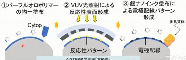
Basic technology of this new manufacturing process is the SuPR-NaP (Surface Photo-Reactive Nanometal Printing) method, which was developed in the past. In this method, first of all, a perfluoropolymers "CYTOP" is coated on the substrate, and then, it's exposed in the intermediary of photo mask by irradiation of VUV light such as wavelength 172 nm. As a result, hydrophobic and hydrophilic pattern is obtained by changing from initial hydrophobic property to hydrophilic property. The next, Nano size Ag ink is coated at pattern-free, as a result, an electrode pattern is completed by adhere of ink to exposed area only.


Pic.1 Porous body and its patterning result
In this new manufacturing process, Nano Ag ink is printed by use of a porous body such as sponges due to correspondence with curved substrate. Concretely, in the last coating process of Nano Ag ink, Ag ink is adsorbed to the porous body, and then, it's contacted to the substrate by transfer printing. In short, capillary phenomenon of the ink is effectively used. As a result, the ink does not bleed. Of course, utilization ratio of main material is high. Therefore, damage against the under layer inclusive of the substrate is not pretty well.

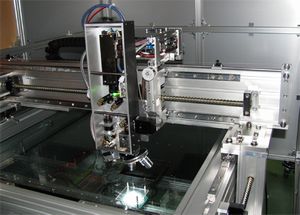
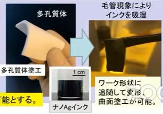
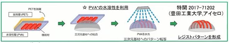
In the research, polyfluoren series were mainly used as a porous body, but other various polymers can be used due to properties such as solvent resistance. And also, a curved photo mask (joint development of Toyota Technological Institute and Aicello) was used. Its cost is not expensive because of repeatable use.

The research group requested to develop a pilot-manufacturing system to Mino Group, which is a printing system maker. Fine pattern same as 9.8 ƒÊm line width is formed on curved substrate (R = 23‡o) by use of this pilot system with robot arms. Its line width uniformity is 2 % and under. And also, it's firmed to be possible to correspond to convex structure and concave structure. Furthermore, the tact time was relatively high same as approximate 5 min.


Fig.2 Manufacturing process flow of curved photo mask

In this process, it's possible to use other various materials as an ink. Firstly, fine P3HT pattern could be obtained such as 25 ƒÊm line width for example, organic solar cell and organic transistor. In addition, in case of curved substrate with array ditch pattern in advance, CYTOP and its VUV process are not necessary, as a result, an ink can be directly printed patterned.


REMARK
STELLA NEWS SITE is a free news site of FPD and PCB by Stella Corporation Inc.(This company does not release these FPD and PCB related products.)

Stella's repair systemgRepair Visionh is suitable for repair use of electrode and so on. Also, it's possible to directly pattern ITO, metal, CNT (Carbon Nano Tube) films by use of this system, too.