|
STELLA NEWS SITE is managed by Stella Corporation Inc. |

The 83rd JSAP Autumn Meeting, 2022 (September 20 - 23) |
|||||||||||||||||||||
September 20 - 23, The 83rd JSAP Autumn Meeting, 2022 was held in Tohoku
University and the online. Topics of OLED, oxide-TFT, organic-TFT and perovskite
solar cell are closed up based on the proceeding.
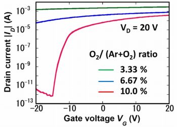
Figure 1 shows transfer characteristics of IGZO-TFTs fabricated under different O2/(Ar+O2) ratio. In both device with O2/(Ar+O2) ratio 3.33 % and 6.67 %, drain current was slightly modulated by gate voltage, but it was 10μA and over in this voltage region. On the other hand, in the device with O2/(Ar+O2) ratio 10 %, general transfer curve was obtained. And also, its carrier mobility in saturation region was 14.5 cm2/Vsec. This is reason why IGZO film became to be semiconductor property because of decrease of oxygen defect in this film by increase of O2/(Ar+O2) ratio in sputtering process. In the past, the research group reported that in case of the conventional InGaZnO4, if O2/(Ar+O2) ratio is 1 % at minimum, semiconductor property occurred. In short, O2 flow rate in sputtering deposition of In rich IGZO film is necessary to increase to 10 times than that of InGaZnO4 film.
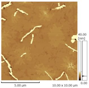
As concerns organic-TFT, the research group of Osaka Institute of Technology and Shizuoka University reported that DNTT with high flatness and crystalline nature was obtained by slow evaporation in the beginning stages of growth. In this experiment, a silicon substrate was washed for 5 minutes by ultrasonic sound using acetone, isopropanol, and pure water, and then, washed by UV/O3 method. DNTT film was evaporated in 10-5 Pa and under. Picture 1 shows AFM image of DNTT thin film. Average roughness (Ra) was greatly flat same as 2.76 nm. As picture, molecular surface terrace structure of DNTT grain was observed. Furthermore, (001) peak in XRD was clearly observed. In short, great flatness and crystallizability of DNTT film was obtained. 2 Color EC device is obtained by use of WO3/NiO multilayers as EC layer With respect to E-paper device, Kitami Institute of Technology reported 2 color EC (electrochromic) device with WO3/NiO multilayers.
In the experiment, WO3 film, NiO film, and ITO film were deposited on glass substrate with ITO transparent electrode by RF magnetron sputtering method. The next, Nafion dispersion liquid was injected into the device as an electrolyte. The device is composed of ITO/WO3/NiO/(ITO)/Nafion/ITO. 2 devices with ITO and without ITO film on NiO film were pilot-produced due to comparison.
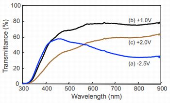
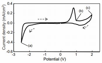
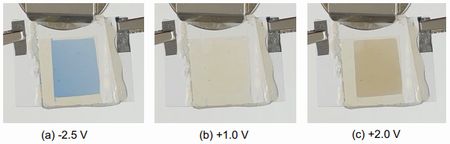
The next, optical characteristics of (a): both films are reduced, (b):WO3 film is oxidized and NiO film is reduced, (c): both films are oxidized were estimated. As figure 4 and picture 2, color is changed to blue at (a), to transparent at (b), and to gray at (C). In short, 2 color EC device confirmed to be gained by use of WO3/NiO multilayers. Characteristics of perovskite solar cell are enhanced by use of SAM as hole transport
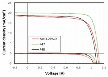
In this research, SAM was adsorbed to glass substrate with ITO transparent electrode as hole transport layer. The next, perovskite film, electron transport film, and bottom electrode were deposited respectively. The conventional carbazole methoxyphosphate (MeO-2PACz), new material F47, and F48 with different substituent groups as SAM material. Their liquids were spin-coated, and then, annealed at 100 ℃ for 10 minutes. As a result, they were adsorbed on ITO electrode. On the other hand, Cs0.05(FA0.83MA0.17)0.95Pb(I0.83Br0.17)3 was used as perovskite material. Figure 4 shows characteristics of pilot-produced device. Compared to device with conventional material (MeO-2PACz), Voc and fill factor (FF) device with F4 were increased, and also, Jsc was slightly increased. Photo resist are highly etched by making use of R-TPJ method
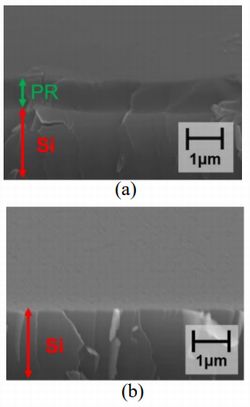
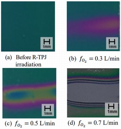
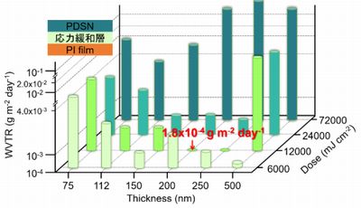
In this experiment, a photo resist was spin-coated on silicon wafer, and then, baked at 130 ℃ for 2 minutes. Picture 3 shows micrographs of photo resist before and (b)-(d) after R-TPJ irradiation. After R-TPJ irradiation, interference color was changed at (b)-(d), and also, surface of silicon substrate was exposed at (d): O2 flow rate = 0.7 L/min Picure.4 shows SEM images of photo resist samples before and after R-TPJ irradiation with O2 flow ratio = 0.7 L/min. Thickness of photo resist film was 1.17 μm before, on the other hand, resist disappeared completely at (d). Considering this result, etching rate is estimated to be 5.85 μm/s and over. Off course, this value is greatly better than that of conventional dry etching method and wet etching method. World highest barrier property in solution-processed barrier film is obtained Yamagata University proposed VUV hardened Perhydropolysilazane (PHPS) film as gas barriers of OLED and organic series solar cell, and reported world highest gas barrier property same as 10-5g/m2/day order (WVTR) in solution-processed gas barrier film.
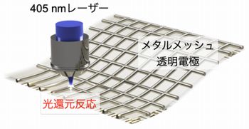
Figure 5 shows WVTR versus PDSN layer thickness (at the VUV dose of 6000 mJ/cm2) and VUV dose. In case of 200nm thickness, VUV dose = 12,000 mJ/cm2, WTVR was 1.8×10⁻⁴g/m2/day at 1 unit structure (PDMS/PHPS). And also, WTVR of 3 unit structure was 4.8 × 10⁻⁵ g/m/day. This value is 2 digits compared to that of the conventional solution-processed gas barrier film. Fine mesh electrode same as submicron is patterned by laser photoreduction method The research group of Shizuoka University announced fine patterned Ag metal mesh electrode as a flexible transparent electrode by laser photoreduction method.
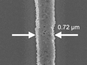
In this process, blue laser (405 nm) is selectively irradiated with laser photoreduction material (film), as a result, Ag ion in irradiated area is reduced. Laser power is 1 - 10 mW, imaging speed is 1 - 1000 μm/s. Picture 5 shows SEM image of fine patterned Ag line. Line width was 0.71 μm, which was invisible by visual contact. Resistance is dicated by laser power and imaging speed. Minimum specific resistance was 2.0 × 10⁻⁷Ω・m in 5mW, 1 μm/s. Reference 1)Nakanowatari, et.al.:Characterization of In5GaZnO10 thin-film transistors, The 83rd JSAP Autumn Meeting, 2022, 16-093 (2022.9) 2)Hiroshiba, et.al.:Growth process of dinaphtho[2, 3-b:2', 3'-f]thieno[3, 2-b]thiophene (DNTT) thin film by slow deposition method, The 83rd JSAP Autumn Meeting, 2022, 11-107 (2022.9) 3)Abe, et.al.:Optical properties of electrochromic devices using WO3/NiO multilayers, The 83rd JSAP Autumn Meeting, 2022, 05-033 (2022.9) 4)Chigira, et.al.:Investigation of self-assembled monolayer (SAM) as the hole transport layers in the perovskite solar cells, The 83rd JSAP Autumn Meeting, 2022, 11-329 (2022.9) 5)Kato, et.al.:Ultra-fast Etching of Photoresist by Reactive Atmospheric-pressure Thermal Plasma Jet, The 83rd JSAP Autumn Meeting, 2022, 07-074 (2022.9) 6)Sasaki, et.al.:Solution-Processed PHPS Gas Barriers with Glass-like Ultrahigh Barrier Performance, The 83rd JSAP Autumn Meeting, 2022, 11-361 (2022.9) 7)Hayase, et.al.:Development of flexible transparent electrode by silver line laser patterning, The 83rd JSAP Autumn Meeting, 2022, 06-003 (2022.9) |
|||||||||||||||||||||
| REMARK STELLA NEWS SITE is a free news site of FPD and PCB by Stella Corporation Inc.(This company does not release these FPD and PCB related products.) |
|