STELLA NEWS SITE is managed by Stella Corporation Inc.

34th INTERNEPCON JAPAN/34th ELECTROTEST JAPAN/21st IC & Sensor Packaging Technology EXPO/21st ELECTRONIC COMPONENTS & MATERIALS EXPO/21st Printed Wiring Boards Expo/10th FINE PROCESS TECHNOLOGY EXPO/12th LED & Laser Diode Technology EXPO (January 15-17, 2020)


NEPCON JAPAN 2019/36th ELECTROTEST JAPAN/20th IC & Sensor Packaging Technology EXPO/20th ELECTRONIC COMPONENTS & MATERIALS EXPO/PWB EXPO/20th Printed Wiring Boards Expo/9th FINE PROCESS TECHNOLOGY EXPO

Shin-Etsu Chemical appealed manufacturing process of micro-LED and its material solutions

January 15-17, 34th INTERNEPCON JAPAN/34th ELECTROTEST JAPAN/21st IC & Sensor Packaging Technology EXPO/21st ELECTRONIC COMPONENTS & MATERIALS EXPO/21st Printed Wiring Boards Expo/10th FINE PROCESS TECHNOLOGY EXPO/12th LED & Laser Diode Technology EXPO were held in Tokyo Big Site. In this here, main topics are picked up.

In LED & Laser Diode Technology EXPO, Shin-Etsu Chemical introduced manufacturing process of micro-LED and its material solutions.


Picture 1. LED chip mounted sample on the glass substrate
GEN
 1st ‚f‚d‚m 2nd ‚f‚d‚m
3rd ‚f‚d‚m
Quartz size
35 ~ 35 mm 
50 ~ 50 mm
4-inch wafer
Quartz thickness
1.2 mm 
1.2 mm
1.2 mm
Silicon base area 29 ~ 29 mm  44 ~ 44 mm 65 ~ 65 mm
Dot area 27 ~ 27 mm  42 ~42 mm 63 ~ 63 mm
Dot size 3 ƒÊm   3 ƒÊm  3 ƒÊm

Table 1. Roadmap of EZ-PETAMP

As concerns this process, first of all, a sapphire substrate with Green or LED chip is assembled with a quartz donor plate, and then, LED chips is transferred to the donor plate by irradiation of laser beam from the sapphire substrate side. The next, the donor plate is washed by making use of HCl and pure water due to elimination of Ga. Subsequently, the donor plate and a stamp (EZ-PESTAMP) with adhesive pattern on the quartz substrate are assembled, as a result, LED chip pattern is transferred to adhesive pattern on EZ-PESTAMP again. Finally, EZ-PESTAMP is contacted with a display glass substrate, as a result, LED chip pattern is transferred to the glass substrate at last.

The company supplies the donor plate and EZ-PESTAMP as a sample. Table 1 shows the roadmap of EZ-PESTAMP. The company is suppling 1G prototype at the moment, but has developed 2G and 3G prototypes yet.

PEDOT is basked in the limelight again as a material of flexible devices


Picture 2. OLED lighting device using PEDOT HIL

Picture 3. Transferred sample
With respect to organic materials for display and lighting device, Heraeus (Germany) appealed a PEDOT gClevios seriesh for flexible device. As you know, PEDOT is a coatable transparent conductive polymer, therefore, it can be used as various transparent electrodes and hole injection material of OLED. As picture 2, an OLED lighting device with Clevios HIL was exhibited in the booth. The company demonstrated that it was adopted in mass production yet.

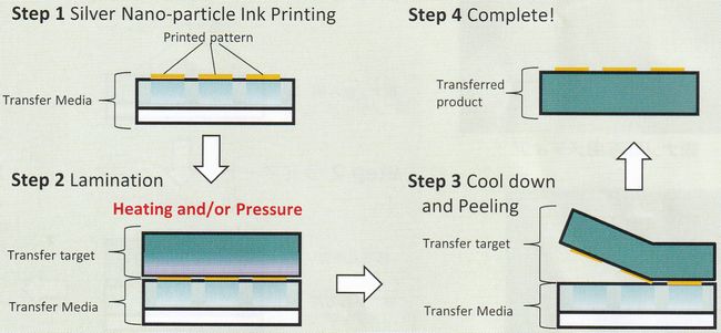
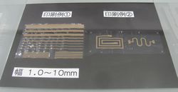
On the other hand, a combined material of PEDOT and Nano size Ag wire (Clevios HY E) was introduced for transparent electrode, too. It has flexibility and high conductance because of properties of PEDOT and Nano size Ag wire. Its surface resistance is 30`150 ƒ¶/ . Furthermore, high durability such as 300 thousand times is obtained in the bending test at R 1mm. By the way, it's difficult to wet-etch PEDOT in general. For this reason, the company recommends an original laser patterning method (‡@A masking pattern is formed on Clevious layer by use of patterned photoresist or printed resist. ‡AClevios layer is patterned by laser irradiation selectively. ‡BMasking layer is eliminated finally).

Sintered Ag pattern at RT is transferred to an actual substrate

On the other hand, Mitsubishi Paper Mills proposed new materials for PCB manufacturing process. One is a Nano size Ag transfer media. Ag pattern is transferred to an actual substrate by transfer process using this media.

Figure 1. Transfer process by making use of Nano size Ag transfer media
As figure 1, first of all, the media is printed by the ink-jet printing method or the screen-printing method. In this time, protective group and solvent composite in the media are absorbed into under layer of the media, as a result, sintered Ag film at room temperature remains on surface at porous state. In short, almost pure Ag film is obtained in this time. The next, the media is laminated to a transfer substrate, and then, released. As a result, Ag pattern is transferred to the substrate. Its sheet resistance is approximate 0.2 ƒ¶/ . By the way, it's possible to increase conductance by use of electroplating method furthermore.

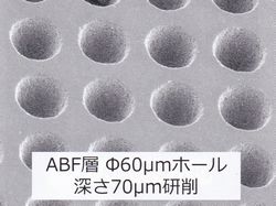
Another is a dry film photoresist (DFR) of the sandblast method for glass substrate and PCB, which is patterned by use of BT (Bismaleimide-Triazine Resin). As you know, high aspect ratio pattern which is difficult by the photo-etching method is obtained by making use of the sandblast method. In this time, the company proposed direct calibration of glass substrate and hole forming process on Cu foil using thick BT resist (50 - 200 ƒÊm) as a masking pattern for effective applications. If this DFR is used in both cases, high aspect ratio and sharp pattern are obtained, too.

Stretchable conductive paste has minimum increase specific resistance at stretch state


Picture 5. Screen printed sample of stretchable conductive paste

Picture 4. Manufactured hole pattern by the sandblast method
Toyo Ink SC Holdings introduced a stretchable conductive paste for flexible devices. Its volume resistivity of standard type and low resistance type are 2 ~ 10-4 ƒ¶¥cm and 3 ~ 10-5 ƒ¶¥cm respectively after curing (80 - 120 Ž). If it is stretched by 20 % and under, its resistance is not almost increased after 10,0000 times, and also, if it returns at initial form, its resistance returns at initial value. It's effective for sensor, actuator, robot, and so on as stretchable conductive material.


REMARK
STELLA NEWS SITE is a free news site of FPD and PCB by Stella Corporation Inc.(This company does not release these FPD and PCB related products.)

Assembly system of emulsion film maskgLCGMh
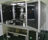
Novel system was released as manufacturing system of emulsion film mask.