STELLA NEWS SITE is managed by Stella Corporation Inc.
STELLA NEWS SITE is managed by Stella Corporation Inc. |
|
Manufacturing process of oxide-TFT 2025 edition |
|
|
Explain TFT structure, and process flow of TFT array, CF array, LC cell, and module assemble. Easy to look at the file using any PC because of the format of browser, for example IE (Internet Explorer) |
|
CONTENT |
||
|
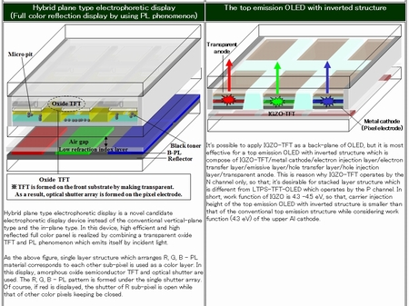
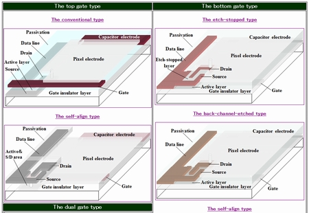
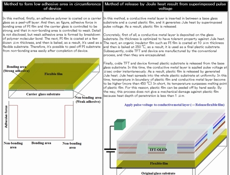
■Categorization and structure of oxide-TFT Categorization of oxide-TFTs The top gate type The bottom gate type The dual gate type ■Manufacturing process of the top gate type (general theory) ■Manufacturing process of the self-align type (general theory) ■Manufacturing process of the back-channel-etched type (general theory) ■Manufacturing process of the etch-stopped type (general theory) ■Manufacturing process of the back-channel-ethed type (The transparent TFT) (general theory) ■Manufacturing process of The dual gate type (general theory) ■Manufacturing process (particular theory) ■A word of caution in manufacturing of oxide TFT with flexible substrate
|
|
|
|
Full-original CD-ROM |
||
|
CD-ROM for Windows & Macintosh
Price:22,000 yen (free shipping) Release date:May 12, 2025 1-1544-7 Kaijincho Minami, Funabashi, Chiba, Japan Zip: 273-0024 Tel: +81-(0)47-432-5031 Fax: +81-(0)47-432-5032 e-Mail support@stellacorp.co.jp https://www.stellacorp.co.jp
|