|
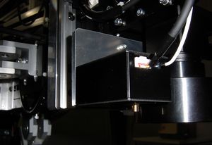
Customized Product Since 1989 our company has established, we have accepted high estimate from users in PCB and photo mask industries because of innovation spirit, low cost ability, original viewpoint, practical result. We invested R&D substantially based on our slogan “Something Special”; in short, our target is different from that of other persons. Our original technology is spread to machine design, electronics circuit design, optics design, development of IC, development of computer software. We have developed these technologies by ourselves. Therefore, we can propose a novel product based on various viewpoints for our users by mass technology in the office. In fact, there were a lot of customized products for specific customers in the past. The next, we introduce its typical examples. Only one probe checker has been developed for automobile affiliated manufacturer In fact, this customer commented that this tool didn’t exist in the probe industry; as a result, we could build out effective inspection framework.
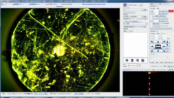
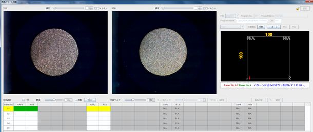
Inspect misalignment of hole and pad on PCB in the both surfaces at the same time Therefore, we aligned two CCD cameras with facing condition, and inserted PCB in between CCD cameras vertically. As a result, in this system, misalignment could be measured and inspected in the both surfaces at the same time. Of course, inspection result can be recorded as enormous data reports by statistical processing. Therefore, user can enhance yield of PCB by making use of this system.
As the above, we have enormous elemental technologies. However, a lot of technologies with ineffective practical use maybe exist. If you search a novel advanced product, please contact with use willingly. Stella Corporation Co., Ltd. |
||||||||||||||