|
STELLA NEWS SITE is managed by Stella Corporation Inc. |

The 69th Japan Society of Applied Physics (JSAP) Spring Meeting 2022 (March 22-26) |
||||||||||
March 22-26, The 69th Japan Society of Applied Physics (JSAP) Spring Meeting
2022 was held by online method. Main topics of electric devices are closed
up based on the proceeding.
Figure 3 shows EQE and angular distributions of electro luminescence. EQE of device B with porous HTL was 32 % at the maximum. As a result, outcoulpring-effieint was increased to approximate 1.4 times by use of porous HTL. Trade-off problem in release process of flexible device is solved With respect to flexible device, the research group of The University of Tokyo reported to optimize release process of flexible device with ultra-thin substrate, which was manufactured by the laser transfer method.
In this experiment, first of all, a fluorine polymer was spin-coated as release layer due to weakening adhesion between glass and palyrene, which became to be a final substrate. The next, palyrene was deposited at 1.5 μm thickness by the CVD deposition method. Figure 4 shows adhesion between parylene and supporting substrate depending on annealing temperature. Adhesion of device without annealing was 0.05 MPa, on the other hand, it was increased to 0.40 MPa by 150 ℃ annealing. In short, trade-off problem in release process could be solved by adhesion control using simple anneal process. ITO electrode of solution-processed oxide-TFT is directly patterned without photoresist, too As regard oxide-TFT, NHK announced new solution-processed electrode using precursor liquid of metallic oxide.
Precursor liquid becomes to be insoluble against etchant by formation of M-O-M bond. If UV light is irradiated, remain solvent is disported, as a result, film density is decreased. In fact, film density was decreased from 3.39 g/cm3 to 3.16g/cm2 after irradiation. For this reason, low dense ITO film can be easily etched. In short, ITO electrode is patterned by making use of difference of solubility between irradiated area and non-irradiated area. The research group developed oxide-TFT with this ITO electrode and sputtering deposited ITZO semiconductor. Its carrier mobility was relatively high same as 15 cm2/Vs at the maximum. Durability of perovskite solar cell is enhanced by O2 plasma treatment Relating to perovskite solar cell, National Institute of Advanced Industrial Science and Technology (AIST) reported that device characteristics were enhanced and manufacturing process time was speeded up by plasma treatment of SnO2 film.
Figure 6 shows J-V curve and parameter. Voc was improved mainly by O2 plasma treatment. Fig.7 shows test result of light resistance. Characteristic of UV ozone treated device was decreased to 80 % compared to initial value after 24h, on the other hand, that of O2 plasma treated device was kept to 90 % after 3000h. In short, light durability is enhanced, and also, treatment process time is speeded up to 40 times by O2 plasma treatment. Characteristics of perovskite solar cell is improved by surface treatment of electron transport layer On the other hand, the research group of University of Electro-Communications and Toin University of Yokohama reported about Ag3BiI6 (Silver Bismuth Halide) perovskite solar cell, an ecological lead-free perovskite solar cell.
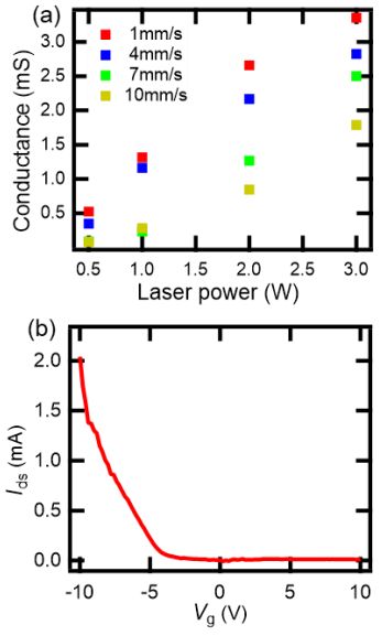
Figure 8 shows change of J-V curve by CsCl treatment. Jsc, Voc, and FF of CsCl treated device were higher these values of non-treated device, and incident photon-to-current efficiency (IPCE) was 2.33 % at the maximum. In particular, Voc of treated device was greatly increased such as approximate 80 mV among 20 test devices. MWCNT electrode is directly patterned by use of laser thermal transfer As concerns carbon nano tube (CNT) electrode, the research group of Tokai University announced laser thermal transfer method, a patterning technology of MW (multi wall) CNT on plastic film directly. In the experiment, first of all, MNCNT dispersion liquid was sprayed on glass substrate. The next, polypropylene film and cover glass were laminated on this MWCNT film. Subsequently, MWCNT film was transferred to surface of PP film by irradiating CW laser (wavelength 450 nm) from glass side at 1 - 10 mm/s, 0.5 - 3.0 W.
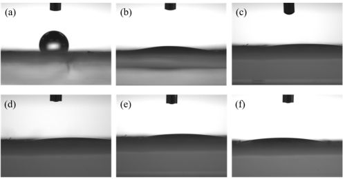
As figure 9-(a), conductive property of this device is increased by decrease of scanning speed and increase of laser power. And also, figure 9-(b), current between drain and source was modulated by gate voltage. In short, it's confirmed that this device was normally functioning as p type FET. By the way, carrier mobility and ON/OFF current ratio were 6.5 cm2/Vs and 1.5×10⁴ respectively. SWCNT film is changed to hydrophilic property by making use of atmosphere plasma treatment By contrast, the research group of Tokai University reported that adhesion between SWCNT film and solder was improved by surface modification of SWCNT film from hydrophobic property to hydrophilic property. In this time, SWCNT powder was dispersed into ethanol by ultrasonic sound, as a result, SWCNT dispersion liquid (0.2 wt%) was prepared. SWCNT film was formed by suck and filtration of SWCNT liquid, and then, it's treated by Ar plasma in atmosphere for 3 sec. Finally, melted solder was adhered to SWCNT film. Picture 1 wettability test of SWCNT films without and with plasma irradiations. Contact angle of water without plasma treatment was 88.4°, on the other hand, it's decreased to 12.8°after plasma treatment, and also, this hydrophilic effect was kept for 4 weeks. Picture.2 shows wettability test of SWCNT film with solder. Compared to with and without plasma irradiation, adhesion of the former was higher than that of the latter. In short, SWCNT film and solder were confirmed to be sufficiently adhered. Reference 1)Aoki, et.al.:Super-low-index porous hole-transport layer for high-outcoupling-efficiency OLEDs, The 69th JSAP Spring Meeting, 2022, 11-030 (2022.3) 2)Sumi, et.al.:Adhesion evaluation between an ultrathin substrate and supporting substrate for transfer integration of ultrathin devices, The 69th JSAP Spring Meeting, 2022, 11-077 (2022.3) 3)Tanaka, et.al.:Development of solution-processed electrode by positive direct patterning, The 69th JSAP Spring Meeting, 2022, 16-026 (2022.3) 4)Yamamoto, et.al.:Stability of Perovskite Solar Cells using Plasma Treatment Electron Transport Layer, The 69th JSAP Spring Meeting, 2022, 11-214 (2022.3)
6)Sugita, et.al.:Nanotube wiring on plastic films by laser thermal transfer, The 69th JSAP Spring Meeting, 2022, 15-037 (2022.3) 7)Miura, et.al.:Improvement and application of wettability in carbon nanotube films using atmospheric pressure plasma jet irradiation, The 69th JSAP Spring Meeting, 2022, 15-141 (2022.3) |
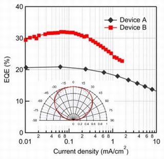
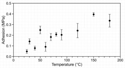
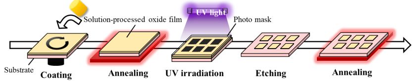
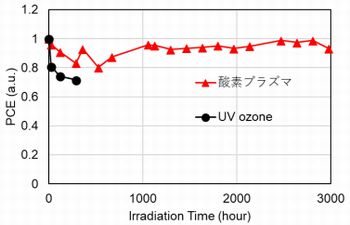
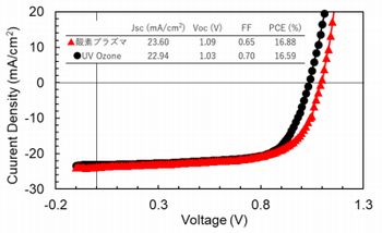
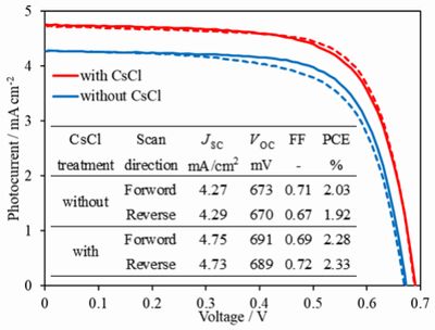 Fig.8 Change of J-V curve by CsCl treatment5)

| REMARK STELLA NEWS SITE is a free news site of FPD and PCB by Stella Corporation Inc.(This company does not release these FPD and PCB related products.) |
|