|
STELLA NEWS SITE is managed by Stella Corporation Inc. |

JST A-SEP ćA New Technology Presentation Meeting (February 25th) |
|||
February 25th, "JST A-SEP ćA New Technology Presentation Meetings"
was held by online method. In this here, two oral presentations about new
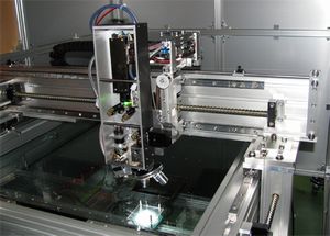
coating technologies are picked up. Prof.(associate) Sakamoto discoursed about flexibly transparent conductive film using Nano size grain, and then, proposed to use this inorganic Nano material as a transparent conductive film.
Furthermore, it's easy to thicken coating film because of high transmittance in visible region at film state, as a result, conductive property can be further enhanced. Of course, its flexibility is sufficient. In fact, after 1000 times of bending test, specific resistance increased mere 10% and under. However, most feature is burning-free. In short, it's possible to form a film by coating only. And also, its material can be patterned by the ink-jet printing method. In a word, it's easy to pattern coated film for transparent wiring. 2D material is simply coated at ultra-thin film Prof.Nagata discoursed about high-speed coating technology of Nano size film using 2D material, and then, reported a new forming process of 2D sheet material (Nano sheet), such as graphene, oxide sheet, and so on. In this here, 2D material is single crystal, which is formed by separation from original strata crystal. Its thickness and xy size are 1nm and a few dozen ā╩m respectively. In this 2D material, new functions such as high-speed electron conduction, high dielectric, and activation of catalyst are expected to be generated. In this process, a drop of dilute choroid water (0.01ü`0.05mg/mL) is dropped on the substrate, and then, suctioned. As a result, the above Nano sheet is obtained easily. Its treatment time is mere 30 sec. In the past, graphene, TiO2, Ru2O, CaNb3, and Cs4W11O16 (photochromic material) have been deposited surely. As you image, it can be deposited on various substrates, such as glass, silicon wafer, plastic film and others because of soft landing process. Furthermore, heat resistance is relatively high same as 80üÄ. And also, adhesive against substrate is practical due to non-peeling in the general peel-off test. By the way, if deposition process is repeated, 3D film and hetero film can be formed by multi-layering. |
|||
| REMARK STELLA NEWS SITE is a free news site of FPD and PCB by Stella Corporation Inc.(This company does not release these FPD and PCB related products.) |
|