|
STELLA NEWS SITE is managed by Stella Corporation Inc. |

36th INTERNEPCON JAPAN/23th IC & Sensor Packaging Technology EXPO/23th ELECTRONIC COMPONENTS & MATERIALS EXPO/23th Printed Wiring Boards Expo/12th FINE PROCESS TECHNOLOGY EXPO (Jan.19 - 21) |
|||||||||||||||
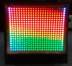
January 19-21, 36th INTERNEPCON JAPAN/23th IC & Sensor Packaging Technology EXPO/23th ELECTRONIC COMPONENTS & MATERIALS EXPO/23th Printed Wiring Boards Expo/12th FINE PROCESS TECHNOLOGY EXPO were held in Tokyo Big Site. In this here, main topics are picked up. Mitsubishi Chemical mounts LEDs on an originally epoxy film
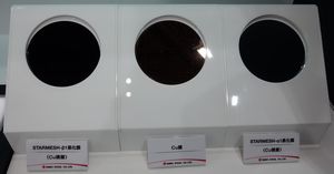
The company exhibited this film firstly at The Total Solution Exhibition for Electronic Equipment 2021, which was held in Tokyo Big Site at October 27-29, 2021, and disclosed a distributed type inorganic EL using this film substrate. In this time, Mini/Micro-LED was exhibited by making use of this film. In short, LED chips were directly mounted on this film with Ag electrode without adhesive layer. As a result, it's sure to be effective for electric devices with high adhesiveness and heat resistance. Reflection ratio is reduced by blackening of wiring using new sputtering target In this time, new proposals about deposition infrastructure were easy to notice. With respect to material, Daido Steel proposed a sputtering target "STARMESH series" as blackening use of Cu wiring for touch-panel of automobile system. and so on. It's possible to greatly reduce reflection ratio because of blackening and suppression of corrosion of Cu wiring by depositing this film on Cu wiring.
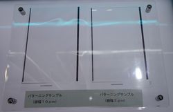
Furthermore, as picture 3, fine patterned samples (10 É m and 3 É m line width) were exhibited, too. In short, it's possible to correspond to fine pattern such as 10 É m and under. In the present moment, the company is supplying sample to deposition makers. Cu film is directly deposited on plastic film by use of high-speed sputtering system
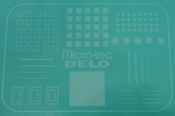
In this system, it's possible to directly deposit Cu film on a plastic film without adhesion layer. It's reason why surface of resin on plastic film is modified because of environment at high density plasma and at medium vacuum area such as 0.1 - 100Pa. In short, function group is generated in surface of plastic film, and then, it's connected to Cu film by chemical reaction. In fact, deposition rate is relatively high same as 35nm/sec. By the way, film thickness uniformity is 10% and under in case of 540 Å~ 630áo substrate. Adhesive is finely patented by the screen printing method As regards manufacturing process, Micro-tec proposed to use the screen printing method for patterning of adhesive. In the booth, printed sample with various shape pattern, such as frame, dot, square, line, entire-surface was pilot-produced by use of the screen printer "MT-650TVC (Micro-tec)" and a specific adhesive (DELO Industrial Adhesives). It's possible to print fine line same as 250 É m width.
|
|||||||||||||||
| REMARK STELLA NEWS SITE is a free news site of FPD and PCB by Stella Corporation Inc.(This company does not release these FPD and PCB related products.) |
| Situation of benchmark test We are testing various treatments in respective lacations by using customer's sample substrate always. Situation of benchmark test is this page. |