|
STELLA NEWS SITE is managed by Stella Corporation Inc. |

Iwate University New Technology Presentation Meeting (July 8th) |
|||||||
July 8th, Iwate University New Technology Presentation Meetings was held
by online method. In this here, two oral presentations based on the i-SB
method are picked up.
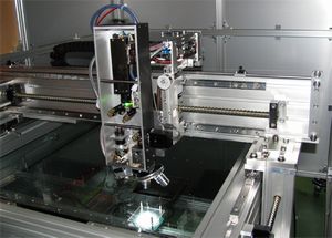
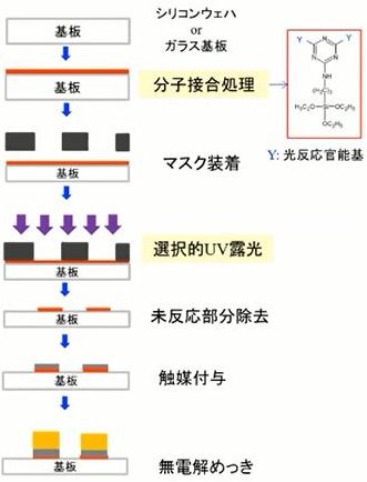
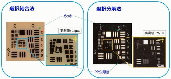
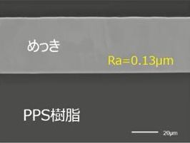
Firstly, direct electrolytic plating on glass and silicon wafer was reported. Its aim is to keep surface flatness of initial value without the conventional anchor technology using roughening procedure. As the above, after molecular bond pattern is formed, firstly a catalyst is selectively adsorbed to molecular bond area, and then, Ni or Cu are selectively plated by the non-electroplating method. Thickness of molecular bond layer was approximate 1.7 nm. In microscope observation, void has not been seen. Surface flatness of glass device was from Ra = 0.9 nm at initial state to Ra = 3.6 nm at after UV irradiation, and also, that of silicon wafer device was from Ra = 0.9 nm at initial state to Ra = 1 nm at after UV irradiation. In short, high surface flatness could be kept after UV irradiation. For this reason, it's possible to satisfy high transfer property, which is required at 5G and 6G device. Furthermore, total process cost can be reduced at 1/2 - 1/3 compared to the conventional photolithography method. It's possible to apply plastic substrate such as PPS resin Subsequently, research result of the i-SB method to plastic molding was reported. Its aim to apply mold interconnect devices (MID), such as multi-function steering, package substrate, antenna, and MEMS sensor.
|
|||||||
| REMARK STELLA NEWS SITE is a free news site of FPD and PCB by Stella Corporation Inc.(This company does not release these FPD and PCB related products.) |
|