|
STELLA NEWS SITE is managed by Stella Corporation Inc. |

SEMICON Japan 2018 (December 12-14, 2018) |
||||||||||||
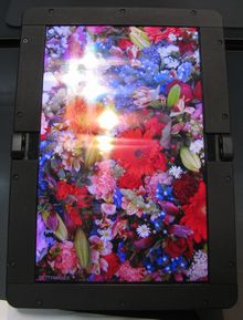
December 12-14, SEMICON Japan 2018 were held in Tokyo Big Site. Main topics of display in this exhibition are picked up. SEL exhibits original OLEDs
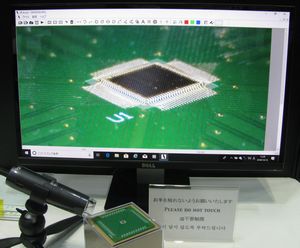
The former is an RGB side-by-side color panel. It was fully flexible by making use of 2 plastic films as both substrates. For this reason, it's possible to bend at Rüü3 ćo. By contrast, the latter is a white EL emission + micro color filter panel because of ultra-high resolution same as 1058 ppi. Concretely, it's composed of tandem units, which were Blue fluorescence emitting unit and Red/Green phosphorescence emitting unit. By the way, original technologies such as OLED materials, CAAC-IGZO (C-Axis Aligned Crystal-In-Ga-Zn-O)-TFT were adopted for both panels. Possible to print in uneven structure by a new screen printing method With respect to manufacturing process, National Institute of Advanced Industrial Science and Technology (AIST) appealed an original printing method "the off-set screen printing method", and also, exhibited a die bond wiring sample, which was formed by this method.
Generally, resolution of the screen printing method is about 50 ā╩m width for mass production, on the other hand, that of the offset screen printing method is W = 20 ā╩m order. Furthermore, in this process, mesh mark of the screen mask does not remain on the substrate by existence of the PDMS blanket. Of course, it's easy to print thick film, too. In this time, AIST pressed that it could be easily corresponded to 3D structure, curved surface, etc. As picture 2, Ag paste was printed on the IC chip at 50 ā╩m width. As a result, it's possible to print Ag paste in side angle of the chip. In short, it can be corresponded to uneven surface easily. This is reason why PDMS blanket is changed by printing pressure, it is synchronized with shape of printing structure. For this reason, it's possible to transfer completely because of without change of ink. High transparent and heat-resistance film appears
|
||||||||||||
| REMARK STELLA NEWS SITE is a free news site of FPD and PCB by Stella Corporation Inc.(This company does not release these FPD and PCB related products.) |
| Stella will run a booth at 36th ELECTROTEST JAPAN which will be held in Tokyo Big Sight on Jan 16 (Wed) - 18 (Fri), 2019. Our booth is E18-16. |