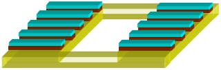
ü®Measure and inspect after development Measuring üĢ AOI inspection system ügST seriesüh
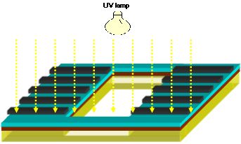
Measure and inspect after exposureü©Measuring üĢ AOI inspection system ügST seriesüh
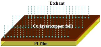
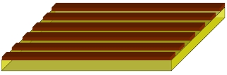
ü®Measure and inspect after etchingMeasuring üĢ AOI inspection system ügST seriesüh
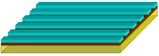
Measure and inspect after developmentü©Measuring üĢ AOI inspection system ügST seriesüh
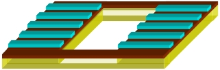
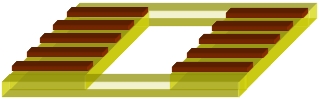
ü®Measure and inspect after strippingMeasuring üĢ AOI inspection system ügST seriesüh
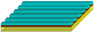
Measure and inspect after etchingü©Measuring üĢ AOI inspection system ügST seriesüh
Stella Corporation Co., Ltd. 1-1544-7 Kaijincho Minami, Funabashi, Chiba, Japan Zip: 273-0024 Tel: +81-(0)47-432-5031 Fax: +81-(0)47-432-5032 e-Mail support@stellacorp.co.jp https://www.stellacorp.co.jp