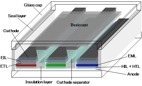
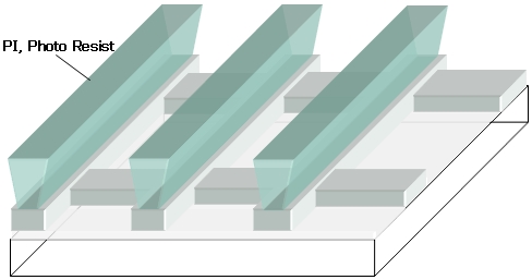
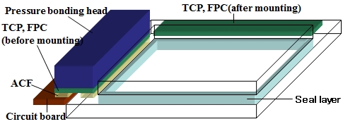
Measure and inspect after development Measuring üĢ AOI inspection system ügST seriesüh
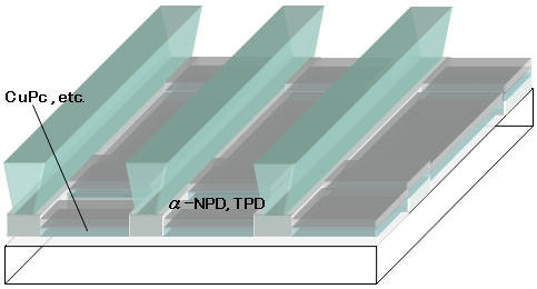
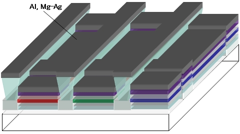
Repair after patterning of anode electrodes Repair system ügRepair Visionüh
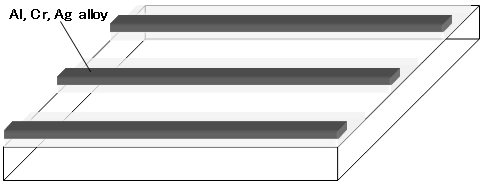
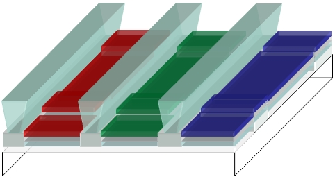
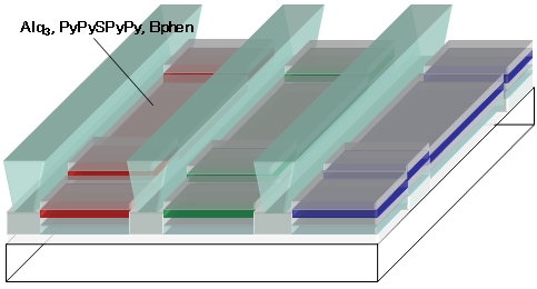
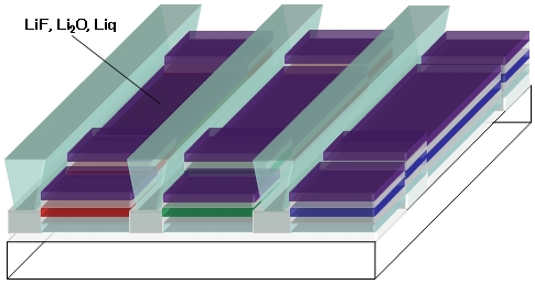
Repair after patterning of metal electrodesRepair system ügRepair Visionüh
Stella Corporation Co., Ltd. 1-1544-7 Kaijincho Minami, Funabashi, Chiba, Japan Zip: 273-0024 Tel: +81-(0)47-432-5031 Fax: +81-(0)47-432-5032 e-Mail support@stellacorp.co.jp https://www.stellacorp.co.jp