|
STELLA NEWS SITE is managed by Stella Corporation Inc. |

The Total Solution Exhibition for Electronic Equipment 2025 (June 4 - 6) |
|||||||||||||||
June 4 - 6th, The Total Solution Exhibition for Electronic Equipment 2025 was held in Tokyo Big Sight. Main topics of display category are picked up. As regards wiring manufacturing process, Nippon Chemical Industrial proposed a CuO2 paste "CURELIGHT" for photo sintering. Its main component is CU2O diameter 100 - 200nm. This paste is printed on substrates by various printing methods, and then, dried at 80℃ due to volatilization of organic solvent. The next, it's reduced to Cu film by irradiation of white light from Xe lamp. Its light sintering time is mere 1 - 3msec. Thermal damage does not occur because of local heating. For this reason, not only polyimide film, but also low thermal resistance substrate such as PET and papers can be adopted. By the way, specific resistance is 20μΩ・cm, which is approximate 10 times than that of bulk. It's possible to print fine line same as 25μm by various printing methods such as screen printing, gravure printing, and flexo printing. In the booth, various printed samples on various substrates were exhibited. It's useful for FPC, touch-panel, electromagnetic shielding, HF/UHF antenna and so on. By the way, it's impossible to print by the ink-jet printing method because of danger of nozzle clogging.
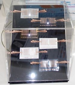
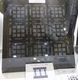
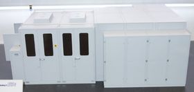
Nippon Electric Glass exhibited 515×510mm TGV (Through Glass Vias) glass core substrates as a next generation semiconductor package substrate. One is patterned glass by laser reforming and etching treatment. Another is patterned glass by irradiation of CO2 laser. Substrate's thickness is 0.4mm or 0.5mm. Fine via hole same as 50 - 90 μm diameter can be formed. By the way, a bare glass substrate without TGV is prepared. The company will mass-produce at 2028. Ultra-fine line same as 1μm is obtained by mask-less exposure As concerns manufacturing system, Ork Manufacturing appealed mask-less exposure system, which was possible to pattern 1μm class line, and then, to pattern Line=1.2μm in spite of using dry film resist (DFR) as result of NEDO (New Energy and Industrial Technology Development Organization) project.
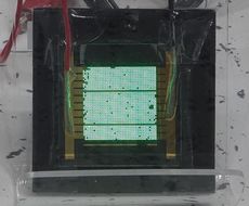
Perfection of Micro-LED with gravure off-set printed solder paste is enhanced Seria Corporation appealed gravure off-set printing machine greatly.
On the other hand, about dot printing of solder paste, a solder paste is printed on 18μm dots in TFT substrate, and then, commercial LED chips are directly mounted on dots by the laser lift-off method, as a result, green Micro-LED was pilot-produced. Perfection of this sample device was enhanced such as great increase of normal turn-on area. |
|||||||||||||||
| REMARK STELLA NEWS SITE is a free news site of FPD and PCB by Stella Corporation Inc.(This company does not release these FPD and PCB related products.) |
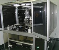
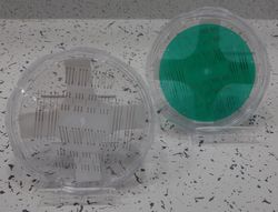
Assembly system of emulsion film mask“LCGM” Novel system was released as manufacturing system of emulsion film mask. |