STELLA NEWS SITE is managed by Stella Corporation Inc.


OPEN HOUSE 2025 (May 28 - June 1, 2025)


OPEN HOUSE 2025 Perfection level of Mini-LED deformable display is enhanced

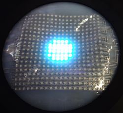
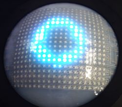
May 28 - June 1, OPEN HOUSE 2025 was held in NHK Science & Technology Research Laboratories. As concerns display, perfection level of Mini-LED using liquid metal electrode were further enhanced.


Pic.2 256~128mm Mini-LED

Pic.1 128~128mm Mini-LED
As above, RGB full-color 128~128 mm (32~32 pixel) and 256~128 mm (64~32 pixel) Mini-LEDs were exhibited as a disformable display, which is possible to change shape at will, like a handkerchief. Dot pitch and LED chip size are 4 mm and 2 mm respectively, and also, resolution was increased 2.5 times compared to the last year exhibits. As picture 1C2, base shape is half-sphere, but it can be changed at will because of rubber sheet substrate with stretchable electrode. As picture 3, bending demonstration was done. As you image easily, its flexibility is higher than that of conventional plastic film device. Furthermore, brightness is relatively high same as 600 - 700 cd/m2.


Pic.3 Bending test
As regards stretchable electrode, which is a key technology of disformable display, in the past, GaIn series was used because of low melting point and function of wiring in spite of liquid metal. In this time, Nanosize Ni grain was doped into this ink, due to suppression of void space and clumping. As a result, uniformly fine line could be printed without void after printing. Of course, this electrode keeps liquid state after painting, and also, functions as wiring at room temperature. Therefore, not only electrode is not broken, but also, its specific resistance is not changed in stretching.

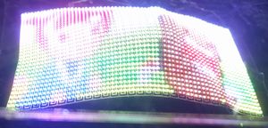
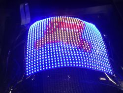
As concerns manufacturing process of Mini-LED display, firstly stretchable electrode is printed on original glass substrate, and then, commercial LED chips are mounted on the electrode. Finally, original substrate is stuck a acrylic rubber sheet, and then, released from original substrate.

Image at LED device is changed in correspond with changed shape of device


Pic.5 Deflated state of LED device

Pic.4 Puffed state of LED device
Furthermore, an unique LED display was exhibited using stretchable electrode, too.

Picture 4 shows puffed state of this LED device, in short, at high specific resistance because of stretched electrode. Picture 5 shows deflated state of LED device with initially low resistance electrode. Image at LED device can be automatically changed in correspond with changed shape of device by configuration of turn on state of LED pixel according as change of specific resistance.

Oxide ITZO-TFT is useful for image device


Pic.6 Bending type image sensor
As concerns TFT, bending type TFT image sensor was disclosed as key device of high view angle camera. It's an oxide-ITZO (In-Sn-Zn-O)-TFT on polyimide film. Manufacturing process temperature is maximum 400 Ž. Practical carrier mobility is obtained almost same as that of conventional IZGO-TFT.

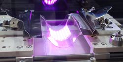
Transparent organic film solar cell is exhibited, too

As regards solar cell, a transparent organic film solar cell was exhibited, too. In this device, non-alkali series electron injection material, which was jointly developed with Nippon Shokubai for inverted structure type OLED. However, composition of this material was not disclosed. Device structure is p-n junction type small molecular device, and their layers were deposited by general evaporation method. In short, it's classic and beginning device, and its incident photon-to-current efficiency (IPCE) is very low same as approximate 1 %.


Pic.8 Application examples of transparent organic film solar cell

Pic.7 Transparent organic film solar cell
However, its transmittance is very high same as 70 % because of effective absorption of UV light. As picture 8, commercial E-paper, pinwheel, and toys were driven by this solar cell, which was generated by solar light and LED lighting in the booth.


REMARK
STELLA NEWS SITE is a free news site of FPD and PCB by Stella Corporation Inc.(This company does not release these FPD and PCB related products.)

One Shot Inspection

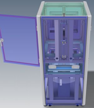
In this system, various patterns in the substrate is captured at 1 shot by the CCD area sensor camera (50 mega-pixel), and then, AOI is treated by original image treatment technologies. AOI time of 320 ~ 420 ‡o substrate is mere 10 seconds.