|
STELLA NEWS SITE is managed by Stella Corporation Inc. |

The 71th Japan Society of Applied Physics (JSAP) Spring Meeting 2024 (March 22-25) |
||||||||||
March 22 - 25, The 71th JSAP Spring Meeting 2024 was held in Setagaya Campus,
Tokyo City University & Online. Topics of OLED, oxide-TFT, and perovskite
solar cell are closed up.
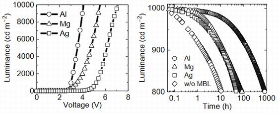
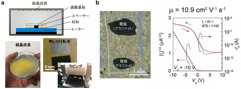
Figure 1-left shows L-V characteristics of produced blue OLED. Device characteristics were in the order corresponding to Al > Mg > Ag. In case of using Al, device was driven at 3V (@1,000 cd/m2) and 4.1 V (@10,000 cd/m2). Work function of stack layer (Al or Mg or Ag/Py-hpp2) were 2.2eV, 2.5eV, and Ag respectively. In short, work function of stacking layer was well correlated with driving voltage. In case of using Al, work function of cathode surface was mere 2 eV because of strong coordination bond of Al and Py-hpp2, and also, electron injection barrier became to be zero. Figure 1-right shows lifetime characteristics at 1000 cd/m2 of initial brightness. Lifetime of OLED was greatly improved by insert of MBL. LT80 lifetime of OLED with Al MBL was 835 h. Furthermore, tandem type OLED with Py-hpp2 interlayer was pilot-produced. Its LT90 lifetime was 1,100 h, which was 7 times compared to that of single device. New process for single crystal organic semiconductor was developed With respect to organic semiconductor, the research group of Institute of Physical and Chemical Research and Tohoku University proposed a new process for single crystal organic semiconductor film such as MT-pyrene, MT-Peropyrene, which were difficult solubility against solvents. As figure 2-(a), indirect sublimation method and transfer method are mixed. Firstly, in the former, single crystals are numberlessly generated on large area in atmosphere environment. The next, it's transferred into the substrate by press, and then, rubbed. As a result, multi-single-crystal films are covered on the whole surface of the substrate. Crystal size is 200 - 300 μm. Organic semiconductor crystal can be completely transferred into the substrate. Figure 2-(b) shows transfer curve of pilot-produced FET (silicon wafer with SiO2 film/CYTOP gate insulator/MT-pyrene organic semiconductor layer/source・drain). Its carrier mobility was 10.9 cm2/Vs. Its approximate 1/3 of that of pure single crystal organic semiconductor device. Its reason why orientation of crystal is random. However, it's higher than that of conventional thin film device in a considerable way.
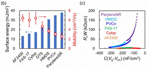
As a result, single crystal is covered on all surface of the substrate. Therefore, uniform single crystal organic semiconductor film was simply obtained on large area. Carrier mobility and Vth of BGBC-OTFT are independent to kind of gate insulator The research group of University of Tokyo and National Institute of Advanced Industrial Science and Technology (AIST) reported relationship of surface energy of gate insulator and contact resistance in bottom-gate bottom-contact (BGBC) type organic transistor.
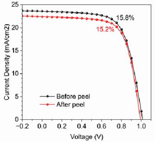
As figure 3, carrier mobility and Vth depends on kind of gate insulator. If surface energy of gate insulator was high, carrier mobility was increased. Furthermore, AF2400, FAS-17 and Cytop with low surface energy were used, contact angle was decreased. In short, injection and transport were confirmed to be influenced by kind of gate insulator surely. Ultra-thin perovskite solar cell with world's highest IPCE was developed With respect to perovskite solar cell, valuable reports have been proposed one after another. Firstly, the research group of Japan Aerospace Exploration Agency (JAXA), University of Tokyo, JST-ACTX, EPFL, and ETH Zurich reported a ultra-thin perovskite solar cell with n-i-p structure. In this here, ultra-thin means full-flexible device with 1 μm order thickness. In this time, sample device could be thin at 1.5 μm thickness, which was world's thinnest record in the field.
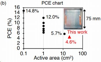
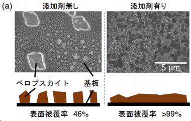
In this device, it's important to devise ITO deposition process due to enhancement of IPCE and durability. Concretely, it's necessary to deposit uniformly amorphous ITO film. Therefore, input sputtering power is increased from 60 W to 120 W in ITO sputtering deposition process. As a result, uniformly amorphous ITO film polycrystal-free was obtained. Furthermore, input power is reduced, and also, treatment time is clipped in O2 plasma treatment due to reduction of plasma damage against perovskite layer. As a result, there is no crack in device at bending state. In fact, pilot-produced device was normally operated at R = 50 μm bending state. As figure 4, high IPCE of pilot-produced device was 18.2 %, which was almost same as that (19 %) of glass device. Its IPCE is world's highest in thin type perovskite solar cell. Deposition method for large-area Sn perovskite is developed As concerns Sn perovskite solar cell, the research group of Kyoto University reported deposition method of Sn perovskite film for large device. In this research, the reduced-pressure drying method was chosen as manufacturing method of Sn perovskite crystal. Crystal growth of Sn perovskite was controlled by making use of a coordinating additive agent. Concretely, a imidazole precursor was used as coordinating additive because of strong cross-interaction against Sn ion in liquid.
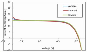
0.1 cm2 device (ITO/PEDOT:PSS/FASnI3/C60/BCP/Ag) was pilot-produced by use of this method. Its IPCE was 7.5 %. Furthermore, large-area 21.6 cm2 device was pilot-produced. Its Voc and IPCE were 3.0 V and 4.6 % respectively. SBI perovskite solar cell with high IPCE same as 13 % was developed By contrast, the research group of Citizen Watch and Toin Yokohama University reported that AgaBibIc (SBI) device with high IPCE was developed as candidate of Pb device.
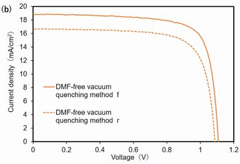
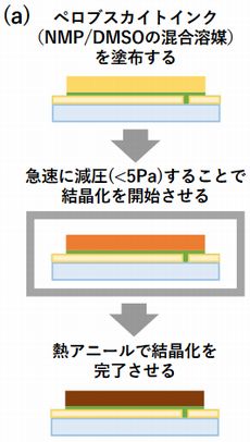
Figure 10 shows J-V curve of pilot-produced device. If Bi is rich in active layer, Voc was greatly improved. And also, durability was enhanced by 3 layer metal electrode (Bi/Cr/Au) due to suppression of interdiffusion. As a result, 2.45 × 2.4 mm device with high IPCE same as 13.25 % was obtained. It means that greatly high value compared to the past record (1.08 %) in SBI device. Perovskite layer is deposited by vacuum quenching method DFM-free AIST proposed vacuum quenching method as fabrication method of perovskite layer.
Its IPCE was 6.01 %. It's greatly lower than that (18 %) of poor solvent method. This is reason why solvent is not completely eliminated in anneal process because of high boiling point of NMP (202 ℃) compared to DMF (153 ℃). For this reason, anneal temperature was changed form 100 ℃ to 150 ℃. As a result, if it's increased, grain size of perovskite was enlarged. However, grain size of 140 ℃ and 150 ℃ was almost same. For this reason, 100 × 100 mm device was fabricated at 140 ℃ in anneal process. High IPCE same as 17.42 % was obtained. Its same as that (17 %) of poor solvent method. Furthermore, 160 × 160 mm device was pilot-produced by making use of slit-coating method and vacuum quenching method. Its characteristics will be estimated in the near future. Degradation mechanism of layers of organic film solar cell is investigated by using high light durability device As regards organic film solar cell, Kanazawa University reported investigation result of degradation mechanism of layers and improvement method of production yield.
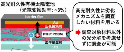
Firstly, an electron transport material ZnO was estimated. After coating by sol-gel method, test devices were annealed by high temperature (250 ℃ × 1h) and low temperature (100 ℃ × 1h). Their initial IPCE was almost same, however, after light irradiation for 100 h, IPCE of the former was 95 %, on the other hand, that of the latter was 74 % compared to initial value. This is reason why if device is annealed at low temperature, active layer is damaged by ZnO film because of rich hydroxyl group on its surface. In fact, resistance of active layer was increased. The next, after UV/O3 treatment of ITO electrode, ZnO film was coated and annealed at 100 ℃ for 1 h. As a result, resistance of active layer was not changed, and also, IPCE was almost same as that of high temperature anneal device. Furthermore, ZnO precursor was coated in vacuum environment (5.0 × 10³ Pa) at 100 ℃ for 5 min. As a result, IPCE was reduced at 5 % only after light irradiation for 100 h. Subsequently, non-fullerene accepter "Y6" was estimated. IPCE of sample device with Y6 and P3HT active layer was reduced at 83 % after light irradiation for 72 h. PEDOT:PSS/Au/barrier film was peeled off, as a result, active layer/ZnO/ITO was remained as a test device due to investigation of its cause. First of all, when Y6 was extracted as liquid state, compared to bulk liquid, its state was not almost different. On the other hand, in AFM observation of test device, its surface was changed, in short, there were a lot of clampings in the surface. By contrast, surface condition of P3HT/ZnO/ITO without Y6 (elimination by dissolution) was not changed. For this reason, Y6 is clamped by thermal damage (light irradiation), as a result, IPCE is reduced. This property is catastrophic weak point for outdoor use, but it's not almost matter for indoor use. On the other hand, with respect to the latter, forming method of top electrode was modified due to improvement of production yield in the top electrode manufacturing process. Concretely, 3 layer structure of metal electrode/thermoplastic resin/barrier layer was prepared. It's laminated on hole transport layer/active layer/electron transport layer/ITO bottom electrode device at 0.8 N/cm2 and 150 ℃ × 5 min. Top electrode is connected with the bottom electrode by the intermediary of through hole, which was manufactured in advance. As a result, tandem module is completed. If this manufacturing process is used, in case of occurrence of NG, this barrier film only is scrapped. On the other hand, in the conventional process, the device inclusive of all layers should be scrapped. IPCE of this device was 98 % of initial state after light irradiation for 100 h. This value was same as that of evaporated Au electrode device and printed Ag electrode device. And also, production yield was improved from 70 % (conventional process) to 100 % in experiment level. By the way, this manufacturing process can be adopted for perovskite solar cell. Reference 1)Sasaki, et.al.:Development of high-performance blue inverted organic light-emitting diodes utilizing coordination reaction with metal buffer layer, The 71th Japan Society of Applied Physics (JSAP) Spring Meeting 2024, 24p-22B-13 (2024.3) 2)Bulgarevich Dmitrievich Kirill, et.al.:Organic Semiconductor “Multi-Single-Crystal Films”:Large Scale Applications of Single-Crystal Devices, The 71th Japan Society of Applied Physics (JSAP) Spring Meeting 2024, 24a-22B-8 (2024.3) 3)Murata, et.al.:Effects of Gate-Dielectric Surface Energy on Contact Resistance in Bottom-Gate-Bottom-Contact-Type Organic TFTs, The 71th Japan Society of Applied Physics (JSAP) Spring Meeting 2024, 24p-22B-3 (2024.3) 4)Jinno, et.al.:Highly Efficient Ultraflexible Perovskite Solar Cells with n-i-p Structure, The 71th Japan Society of Applied Physics (JSAP) Spring Meeting 2024, 24p-22C-7 (2024.3) 5)Harada, et.al.:Development of Thin-film Fabrication Method for Large-area Sn Perovskite Solar Cell, The 71th Japan Society of Applied Physics (JSAP) Spring Meeting 2024, 23p-22C-3 (2024.3) 6)Nakagawa, et.al.:Fabrication of Inverted Bismuth Silver Iodide Solar Cells, The 71th Japan Society of Applied Physics (JSAP) Spring Meeting 2024, 23p-22C-7 (2024.3) 7)Araki, et.al.:Fabrication of perovskite solar cells by DMF-free vacuum quenching method, The 71th Japan Society of Applied Physics (JSAP) Spring Meeting 2024, 24a-22C-3 (2024.3) 8)Nakano:Improvement of Durability and Production Yield of Organic Solar Cells, The 71th Japan Society of Applied Physics (JSAP) Spring Meeting 2024, 22p-22C-1 (2024.3) |
| REMARK STELLA NEWS SITE is a free news site of FPD and PCB by Stella Corporation Inc.(This company does not release these FPD and PCB related products.) |
|