|
STELLA NEWS SITE is managed by Stella Corporation Inc. |

NEPCON JAPAN 2018/35th ELECTROTEST JAPAN/19th IC & Sensor Packaging Technology EXPO/19th ELECTRONIC COMPONENTS & MATERIALS EXPO/PWB EXPO 19th Printed Wiring Boards Expo/8th FINE PROCESS TECHNOLOGY EXPO (January 17-19, 2018) |
|||||||||||||||||||||||||||
January 17-19, NEPCON JAPAN 2018/35th ELECTROTEST JAPAN/19th IC & Sensor Packaging Technology EXPO/19th ELECTRONIC COMPONENTS & MATERIALS EXPO/PWB EXPO 19th Printed Wiring Boards Expo/8th FINE PROCESS TECHNOLOGY EXPO were held in Tokyo Big Site. In this here, main topics are picked up.
First of all, as concerns a flexible device, Ajinomoto Fine-Techno appealed a transparent adhesive barrier film against water vapor. For example, if it is used as a gas barrier film for OLED and organic film solar cell, it is laminated on the rear substrate with device, and then, this rear substrate is encapsulated by another front substrate. Film thickness of thermal curing type is 5 - 50 ā╩m, and that of UV hardening type is 10 - 50 ā╩m.
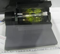
Table 1 shows elapsed time for penetration of water vapor from edge to 5 ćo depth. As table 1, its gas barrier property was 30 - 100 times compared to that of the reference. Of course, light transmission is 98 % and over. Furthermore, in case of 100 thousand time bending test at R = 30 ćo condition, device property was not changed because of superior flexibility. In the booth, 100 ü~ 100 ćo size monocolor OLED which was pilot-produced with Institute of Systems, Information Technologies and Nanotechnologies (ISIT) was exhibited at bending state as picture 1. By the way, its gas barrier property is sufficient for quantum dot display, E-paper display, and organic film solar cellüCon the other hand, it is not sufficient for OLED, which is necessary to have higher gas barrier property. For this reason, if it is used for OLED, first of all, gas barrier thin film is deposited on OLED device by the CVD method, and then, this film is laminated on the device. Visibility of in-car monitor is enhanced by use of ultra-low reflection film
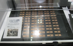
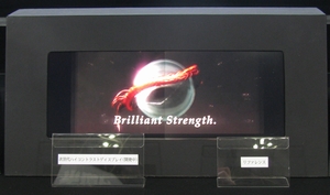
As regards infrastructure for display, AGC demonstrated a new ultra-low reflection film. This film is a polycarbonate film with original anti-reflection function. Its reflection rate is mere 0.099 %. If it is built in monitor for automotive, visibility is not only greatly enhanced, but also, bright contrast ratio and black level are increased by prevention of reflection to the front glass. As picture 2, in the booth, demonstration was done by in-car monitor. Difference of visibility among new product and the reference was defined. Low temperature curing type Cu paste for the screen printing appeared on the scene In respect of electric paste, NOF Corporation announced development of Cu paste for the screen printing. In spite of general grain size (approximate 5 ā╩m), it is fired at low temperature in atmosphere environment. In case of 120 üÄ firing, specific resistance is 30 ā╩āČźcm, in case of 180 üÄ firing, that is 20 ā╩āČźcm. Of course, it has high humidity resistance; as a result, migration does not almost happen for wiring use. And also, it is corresponded to various substrates, such as PET, ceramic, paper, and cloth. Furthermore, it is used for not only the conventional flat screen printing, but also, rotary screen printing and cylinder press screen printing. In fact, various samples with these substrates and printing methods were exhibited in the booth. Antifouling property and pattern resolution of photo mask are improved by hard coated mask with ultra-thin protective film
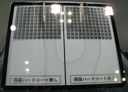
On the other hand, System Advance exhibited an original photo mask with hard coated protective film. In this photo mask, an original silicon resin is coated on surface of photo mask at ultra-thin film. As a result, antifouling property is greatly improved. Picture 4 shows comparison of hydrophobic property by drop of water. In case of this hard coated photo mask, hydrophobic property was greatly enhanced. And also, in the contact exposure process, light leak is reduced by ultra-thin prospective film (10 nm thickness); as a result, exposure resolution and patterning repeatability are surely enhanced. Same as the conventional photo mask, it can be corresponded to 800 ü~ 800 ćo at maximum. |
|||||||||||||||||||||||||||
| REMARK STELLA NEWS SITE is a free news site of FPD and PCB by Stella Corporation Inc.(This company does not release these FPD and PCB related products.) |
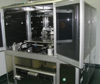
Novel system was released as manufacturing system of emulsion film mask. |