|
STELLA NEWS SITE is managed by Stella Corporation Inc. |

27th FINETECH JAPAN/8th FilmTech Japan (April 5-7) |
|||||||||||||||||||||
April 5-7, 27th FINETECH JAPAN/8th FilmTech Japan were held in Tokyo Big Sight. Main topics in these exhibitions are picked up. First of all, with respect to display module, BOE Technology (China) exhibited display modules alone. Main model is 8K 98 inch TFT-LCD, which is released already. Its large size and high resolution had a great presence. However, this module was exhibited 2 years ago, so that showed no originality. Quality of tiling type OLED is enhanced by transparent frame part in the panel
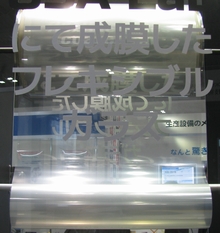
On the other hand, Semiconductor Energy Laboratory demonstrated some OLEDs, which were driven by an original oxide-TFT CAAC-IGZO (C-Axis Aligned Crystal-In-Ga-Zn-O) -TFT. Main exhibition was curved multi display, which was made by tiling of flexible panels. As picture 1, multi display which was made by tiling of 3 panels (14.5 inch) for car system use was demonstrated. In this display system, seem area between panels was not easy to notice by use of transparent frame (widthüü5ćo). In fact, seem area was not recognized from far of 50 cm and over. In this panel, RGB independent emitting method was adopted by use of blue fluorescence and Red and Green phosphorescence materials. As regards manufacturing process, first of all, CAAC-IGZO-TFT and OLED were manufactured on an original glass substrate, and then, it was encapsulated by coating of resin. The next, it was released from this original substrate by making use of function of release layer, and then, released device was transferred to TAC film. For this reason, its thickness is mere 0.1 ćo, and flexible characteristic was excellent such as Rüü2ćo. By the way, vapor permeability of this panel was low such as 10-6g/m2/day order (WVTR). This value is almost same as that of the conventional glass panel. Thermal resistance of basic film is improved by an original adhesive layer
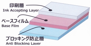
As concerns materials, Nippon Paper Industries proposed a unique plastic film for printed electronics use. As figure 1, this film is composed of basic plastic film, printing layer, and anti bloking layer. The company supplies this film to device makers for example touch panel makers. Printing layer functions as an adhesive layer against printing ink and paste, and it is not absorbing this ink and paste. However, as a result, it's possible to print fine line at low bleeding by use of this film. Furthermore, its thermal resistance is superior such as 210 üÄ order. In short, thermal resistance of basic film can be increased in essence. This means that firing temperature of ink and paste are able to be increased. In fact, characteristics such as electric conductance of device can be enhanced. For this reason, it's hopeful for low-cost plastic film with low thermal resistance as alternate film of polyimide film, which is used as a high thermal resistance film. Picture 3 shows some printed samples of the screen printing, the gravure printing, and the ink-jet printing. In short, this film can correspond to various printing methods. Moreover, it can correspond to not only heat annealing process, but also, light annealing process. In fact, the company appealed that if the light annealing process is adopted on PET film, there is possibility of caving by damage; on the other hand, there is not possibility of caving because of damage free. Thin film encapsulation layer is thinner by use of ALD film
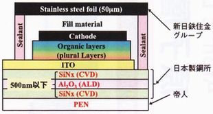
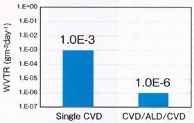
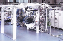
As respects manufacturing system, The Japan Steel Works introduced ALD (Atomic Layer Deposition) system for thin film encapsulation of OLED. If ALD process is used, high encapsulation characteristic is gained because of high density film and excellent step coverage. In this regard, single layer of ALD deposited Al2O3 film or SiOx film is insufficient for encapsulation of OLED, so that, the company proposed 3 multi-layer of CVD deposited film/ALD deposited film/CVD deposited film. Thickness of CVD deposited film and ALD deposited film are 100 nm and under, 20nm and under respectively. In this structure, as figure 2, low vapor permeability such as 10-6g/m2/da is gained. Picture 4 shows a flexible OLED lighting device with this 3 layer gas barrier films on PET film. Flexible characteristic of this device is superior compared to the conventional organic and inorganic hybrid layers because of thinner film. In fact, if it is bent at Rüü30ćo condition, encapsulation characteristic is not almost degraded. The company has developed a cluster tool type system inclusive of CVD deposition chamber. This system can correspond to 6th generation substrate at a maximum. By the way, deposition rate of ALD process is 3 - 5nm/s. Roll to Roll type deposition system for flexible glass appeared on the scene
Von Ardenne (Germany) appealed infrastructure for flexible roll glass, which is proposed from glass makers, for example Nippon Electric Glass, and introduced Roll to Roll type pilot deposition system FOSA LabX 330 GLASS for various functional films. Flexible glass with deposited ITO film (thicknessüF150nm) by this system was exhibited, too. It's possible to correspond to sputtering process, PE-CVD process, and evaporation process, and to use the conventional planar target and rotary target in the sputtering process by use of this system. |
|||||||||||||||||||||
| REMARK STELLA NEWS SITE is a free news site of FPD and PCB by Stella Corporation Inc.(This company does not release these FPD and PCB related products.) |
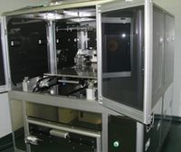
Novel system was released as manufacturing system of emulsion film mask. |