|
■Structure of a-Si TFT-LCD
■Liquid crystal material and display mechanism
■TFT array process
Etch-stopped layer type
Back-channel-etched type (5 masks)
Back-channel-etched type (4 masks)
Forming process of gate electrode
Forming process of gate insulator film, a-Si film, and etching stopper film (Etch-stopped layer type)
Forming process of a-Si island, S/D electrode(Etch-stopped layer type)
Forming process of data line and S/D electrode
Forming process of passivation layer and contact hole
Forming process of pixel electrode
Forming process of gate insulator film, a-Si, n+ a-Si layer (Back-channel-etched type:5 mask)
Forming process of S/D electrode, n+ a-Si island (Back-channel-etched type:5 mask)
Forming process of gate insulator film, Si channel, and S/D electrode (Back-channel-etched type:4 mask)
■CF (Color filter) forming process
Manufacturing process of CF for IPS mode/FFS mode TFT-LCD
Manufacturing process of CF for VA mode TFT-LCD
Manufacturing process of CF for TN/OCB mode TFT-LCD
Black matrix forming process
Manufacturing process of R, G, B color layer
Manufacturing process of overcoat layer
Deposition process of opposite electrode
Manufacturing process of post-spacer
Manufacturing process of rib (bump)
Photo-alignment process (for MVA mode TFT-LCD)
■LC cell process
Polyimid coating process
Alignment process
Seal layer forming process
Dispersion process of spacer-ball
Making panel thinner process
Scribe and break process
Filling process of LC material
ODF (One drop fill) process
■Module assemble process
Connect panel and driver-IC
■Structure of backlight module
Side light type
Light guide plate technology
Structure of direct type
LED backlight for TV (Direct type, side light type)
■3D technology
Method to use a specific glasses
LC shutter glasses method (Time sequential method)
Polarized glasses + patterned phase difference film (Space division method)
Specific glasses-free method
Parallax barrier method
Parallax barrier using dual emission OLED
Time sequential driving + parallax LC barrier method
Lenticular lens method
Time sequential twin-lens 3D-OCB method
Lenticular + time sequential scanning backlight method
|
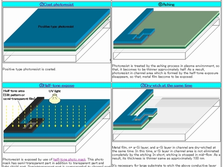
▲Process flow of 4 PEP a-Si TFT
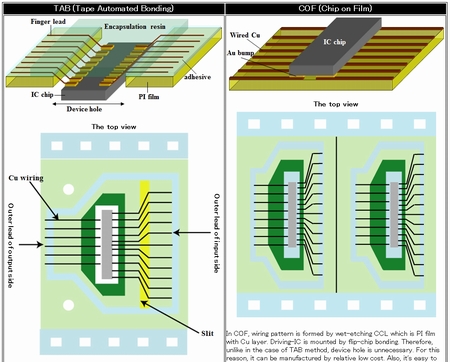
▲Structure of TAB and COF
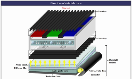
▲Structure of BL module
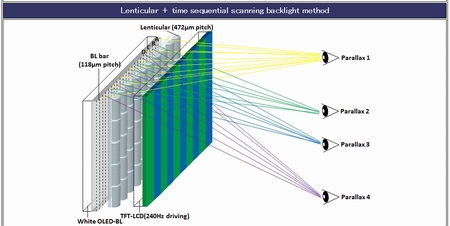
▲3D technology sample
|

